SLLA621A September 2023 – October 2023 MCF8315A , MCF8316A
2.2.3 Solve the Thermal Challenges From PCB Layout
PCB layout also has a large impact on thermal performance. The following example shows that the temperature difference between a good layout and a poor layout can reach 15°C.
- For systems without heat sinks, the heat dissipation on the chip can be improved with larger copper pours. Choose 2 oz. or more of copper thickness as much as possible, which greatly help heat dissipation. However, larger copper pours also mean more cost, so system requirements need to be accounted for when choosing copper thickness.
- MCF831x has Thermal Pad, we need to use MCF831x as much as possible to dissipate the heat through the common. Note it is important to transfer heat to other PCB layers through as many vias as possible. (As shown in Figure 2-11, the PCB on the right is better).and open solder mask in the vias, which help transfer the heat of the MCF831x through the thermal pad to the copper on the PCB. And use multi-layer boards as much as possible to provide more heat dissipation area.
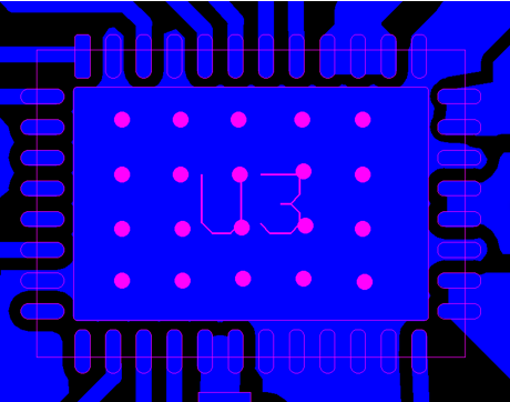 Figure 2-11 MCF831X PCB With Few Vias
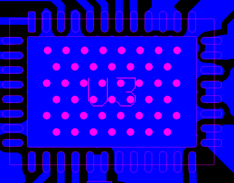 Figure 2-12 MCF831X PCB With More Vias
In the Top layer, connect the pins with the Thermal pad as much as possible to transfer the heat out through them.
Thermal pad connection to a solid copper plane is an important requirement to create a heat dissipation path. For heat to flow away from the device, the copper plane must be continuous. Connect thermal pads to other areas on the board. The best practice is to include wide exit paths in the copper fill. Create a wide, high-surface-area plane below the driver. If these planes are interrupted, the heat dissipation path is shrunk, thereby increasing the thermal resistance. An increase in thermal resistance produces a greater temperature difference between the thermal pad and a wider surface area on the same plane.
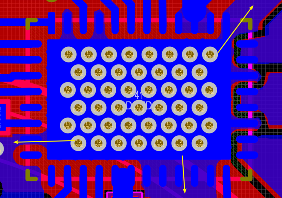 Figure 2-13 MCF831X Heat Dissipation Path (Bottom Layer)
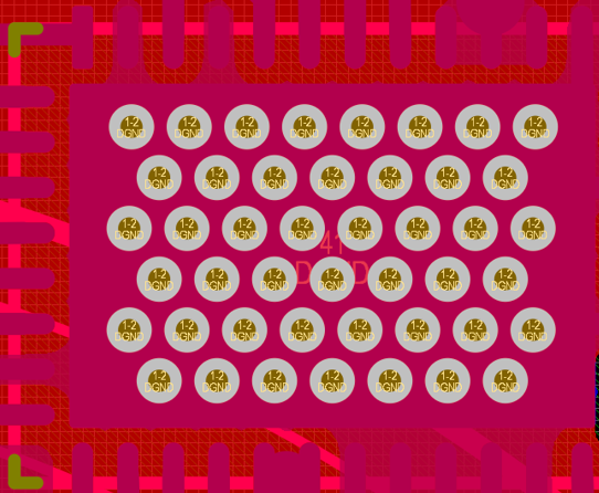 Figure 2-14 MCF831X Heat Dissipation Path (Top Layer)
Figure 2-15 shows a thermal simulation; optimizing the PCB layout reduces the overall temperature rise by 15°C.
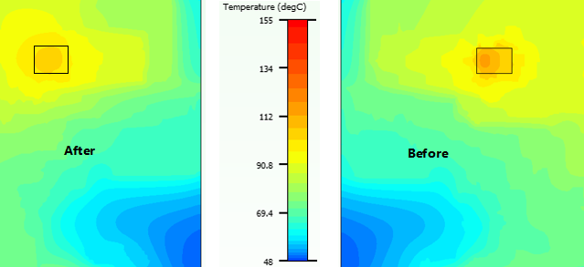 Figure 2-15 Thermal Simulation for MCX831X Layout