SLLA623 September 2023 THVD8000 , THVD8010
2 What is Powerbus?
Before any comparison between Classical RS-485 and Powerbus can occur, a thorough understanding of the theoretical underpinnings of TI’s Powerbus is required. First a look into the OOK modulation scheme, as well as, the physical modulator and demodulator shows how the data is encoded and decoded. Then a look into the physical transceiver and how the transceiver operates on the bus. Finally, a look into the external coupling network and the function the network serves.
OOK modulation, which is also known as On-Off Keying, is the simplest form of Amplitude Shift Keying (ASK) which represents digital data with the presence or absence of a carrier signal. In TI’s Powerbus this is taken a little farther by taking lower speed digital data transmissions and sending out a higher frequency (at least 10 times the data-rate) OOK modulated signal where the presence of the carrier signal indicates a logic low (binary value 0) and the absence of a carrier signal indicates a logic high (binary value 1).
| Input Bit | Powerbus OOK Output | Powerbus OOK Input | Output Bit |
|---|---|---|---|
| 0 | Carrier Active at Modulation Frequency | Carrier Active at Modulation Frequency | 0 |
| 1 | Bus Idle – No Carrier Active | Bus Idle – No Carrier Active | 1 |

 Figure 2-1 THVD80x0: Modulation and Demodulation
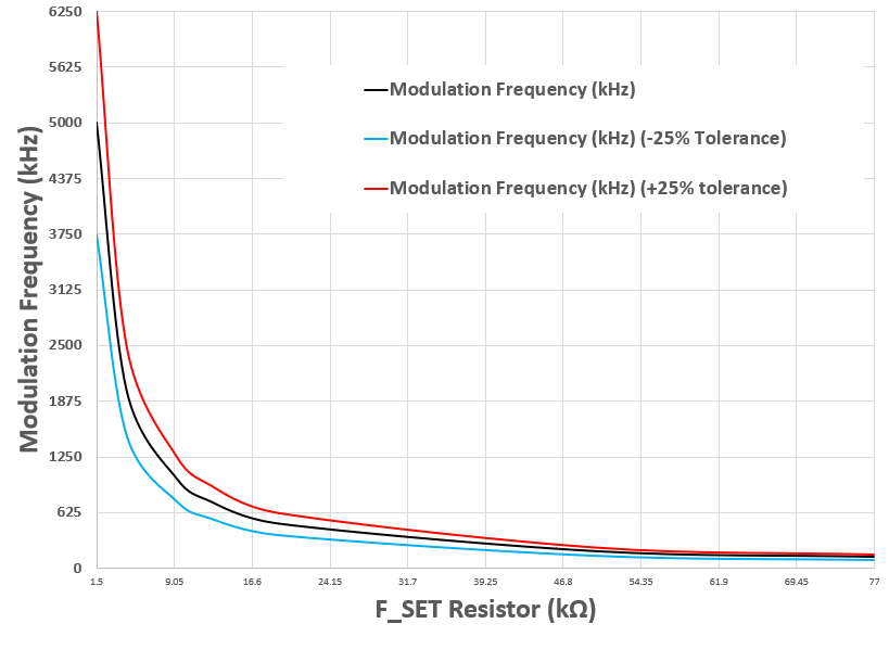
Modulation frequency is chosen via a setting resistor on the THVD8000 or THVD8010. The THVD8000 can have a modulation frequency from 125kHz to 5MHz while the THVD8010 is from 125kHz to 300kHz, but is less sensitive to noise than the THVD8000.
 Figure 2-2 THVD8000 Modulation Frequency v. Setting Resistor Value
Demodulation of OOK signals follows the same logic as modulating the signal but in reverse. The demodulator does this by using an integrated variable frequency bandpass filter, controlled via the same setting resistor as before so that is best primed to receive data at the correct frequency. One important nuance here is that the variable bandpass filter has a low-quality factor (Q0) value which means its passband is wide – this is done because the modulator itself has a ±25% tolerance on the carrier frequency of the signal alone – so the filter itself is not the most selective and using multiple OOK frequencies on one bus can result in communication issues and is not generally advisable.
With an understanding of the modulator and demodulator; the transceiver itself can be looked at in more detail.
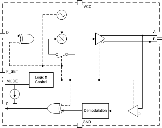
 Figure 2-3 THVD80x0: Functional Block Diagram
The functional block diagram shows that Powerbus devices can be broken down into three groups. First, the digital console facing pins (D, MODE, and R) which control the device and allow for transmission to and from a controller of the transceiver. The D and MODE pins are standard logic inputs that follow other logic inputs common to Classical RS-485 devices – an input high is 2V or greater, an input low is 0.8V or less. D is the transmitted data and MODE is the control of the device – where a logic high can put the device into transmit mode while a logic low can put the device into receiver mode. Second is the modulator and demodulator – this is where the OOK modulation and demodulation scheme are physically integrated into the part, they function as previously described. Finally, the actual transceiver bus facing pins A and B. This front end is RS-485 compliant in everything except its input thresholds (due to the modulation scheme) so it won’t negatively impact a Classical RS-485 bus – but it will not be able to communicate with the other devices on the line.
Arguably one of the most important aspects of Powerbus design is the external coupling network – as this is what allows power and data to transmit on the same bus.
 Figure 2-4 THVD80X0 Simplified Schematic (THVD8010 Shown)
Each node’s coupling network consists of 2 capacitors and 2 inductors. In the simplified THVD80X0 schematic with THVD8010 shown has C1, C2, L1, and L2 represent the first THVD8010’s coupling network while L3, L4, C3, and C4 represent the second THVD8010’s coupling network. At a high level the idea behind the shared bus is that of Frequency Division Multiple Access (FDMA) – where the data signal is at a much higher frequency than that of the power signal (which is either going to be 0Hz (DC) or low frequency AC (50Hz – 60Hz)) and the intended load for each target can filter the unwanted signal out. In practice this means the capacitors in the network should be low impedance to the THVD8000 or THVD8010 but high impedance for the power signal to allow the transceiver to only interact with the data signal itself. Conversely the inductors need to be low impedance for the power signal to conduct through without much attenuation while being high impedance to the OOK data signal to prevent the transceiver from being overloaded and to help prevent noise on a power source or load. It is assumed the power sources and power loads have bulk capacitance to help create an AC ground for the OOK signal – this is an important consideration when working with AC power supplies versus the simpler DC power supplies. The capacitors and inductors are sized according to the following equations which assume the system is properly terminated (two 120Ω terminations, one at each end node).
The capacitor sizing sets the capacitor to be at 5 Ω at modulation frequency for the minimum allowable capacitance on each node. If this process is not followed, the data signal can suffer from higher attenuation. This value can be lower than 5 Ω, but not higher.
The inductor sets the minimum effective inductance value per inductor used (for example, if you had 2 nodes and 4 inductors each one needs at least LMin). N is the number of other Powerbus nodes on the same bus. For small values of N, the inductance value is not affected by transceiver loading that strongly, but as N grows larger, it becomes an important part of the calculation. This keeps the common mode loading of the bus to be equal to or greater than 375 Ω which represents the approximate common mode loading of 32 Unit Loads – which is the maximum allowable by RS-485. This equation only gives the effective inductance – as the power supply current can cause derating – it is critical to make sure the effective inductance is at this level during operation. Other inductor parameters are determined by the power system needs – not that of the THVD8000 or THVD8010.
The coupling network ultimately works as a filter while the modulation scheme is the one that allows robust communication on the same line as a power signal. This network is not needed for the THVD8000 or THVD8010 to operate, but to protect itself from potentially damaging power signals and preventing bus overload.
This is not an exhaustive list of potential modifications with Powerbus, but the list does show the basic design principle behind a standard Powerbus application.