SLLSES1D December 2015 – September 2020 HD3SS3220
PRODUCTION DATA
- 1 Features
- 2 Applications
- 3 Description
- 4 Revision History
- 5 Pin Configuration and Functions
- 6 Specifications
-
7 Detailed Description
- 7.1 Overview
- 7.2 Functional Block Diagram
- 7.3
Feature Description
- 7.3.1 DFP/Source – Downstream Facing Port
- 7.3.2 UFP/Sink – Upstream Facing Port
- 7.3.3 DRP – Dual Role Port
- 7.3.4 Cable Orientation and Mux Control
- 7.3.5 Type-C Current Mode
- 7.3.6 Accessory Support
- 7.3.7 Audio Accessory
- 7.3.8 Debug Accessory
- 7.3.9 VCONN support for Active Cables
- 7.3.10 I2C and GPIO Control
- 7.3.11 HD3SS3220 V(BUS) Detection
- 7.3.12 VDD5 and VCC33 Power-On Requirements
- 7.4 Device Functional Modes
- 7.5 Programming
- 7.6
Register Maps
- 7.6.1 Device Identification Register (offset = 0x07 through 0x00) [reset = 0x00, 0x54, 0x55, 0x53, 0x42, 0x33, 0x32, 0x32]
- 7.6.2 Connection Status Register (offset = 0x08) [reset = 0x00]
- 7.6.3 Connection Status and Control Register (offset = 0x09) [reset = 0x20]
- 7.6.4 General Control Register (offset = 0x0A) [reset = 0x00]
- 7.6.5 Device Revision Register (offset = 0xA0) [reset = 0x02]
- 8 Application and Implementation
-
9 Layout
- 9.1
Layout Guidelines
- 9.1.1 Suggested PCB Stackups
- 9.1.2 High-Speed Signal Trace Length Matching
- 9.1.3 Differential Signal Spacing
- 9.1.4 High-Speed Differential Signal Rules
- 9.1.5 Symmetry in the Differential Pairs
- 9.1.6 Via Discontinuity Mitigation
- 9.1.7 Surface-Mount Device Pad Discontinuity Mitigation
- 9.1.8 ESD/EMI Considerations
- 9.2 Layout
- 9.1
Layout Guidelines
- 10Device and Documentation Support
- 11Mechanical, Packaging, and Orderable Information
9.1.6 Via Discontinuity Mitigation
A via presents a short section of change in geometry to a trace and can appear as a capacitive and/or an inductive discontinuity. These discontinuities result in reflections and some degradation of a signal as it travels through the via. Reduce the overall via stub length to minimize the negative impacts of vias (and associated via stubs).
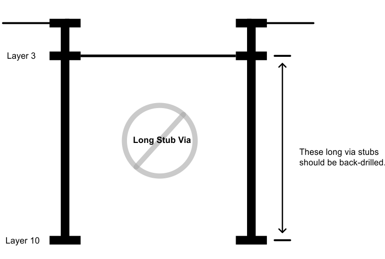
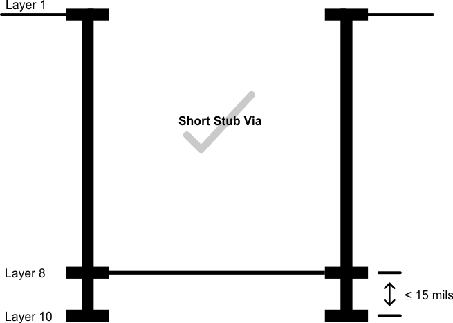
Because longer via stubs resonate at lower frequencies and increase insertion loss, keep these stubs as short as possible. In most cases, the stub portion of the via present significantly more signal degradation than the signal portion of the via. TI recommends keeping via stubs to less than 15 mils. Longer stubs must be back-drilled. For examples of short and long via lengths, see Figure 9-5 and Figure 9-6.
 Figure 9-5 Via Length (Long Stub)
 Figure 9-6 Via Length (Short Stub)