SLOA284A january 2020 – may 2023 AFE5832 , AFE5832LP , ISO7741 , ISOW7841 , LM25037 , LM25180 , LM5180 , LM5181 , LM5181-Q1 , TX7316 , TX7332
3.2 Output Ripple Measurement
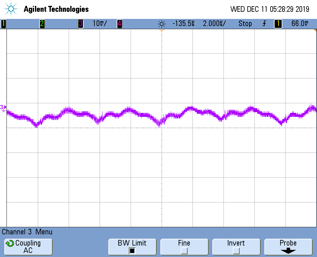
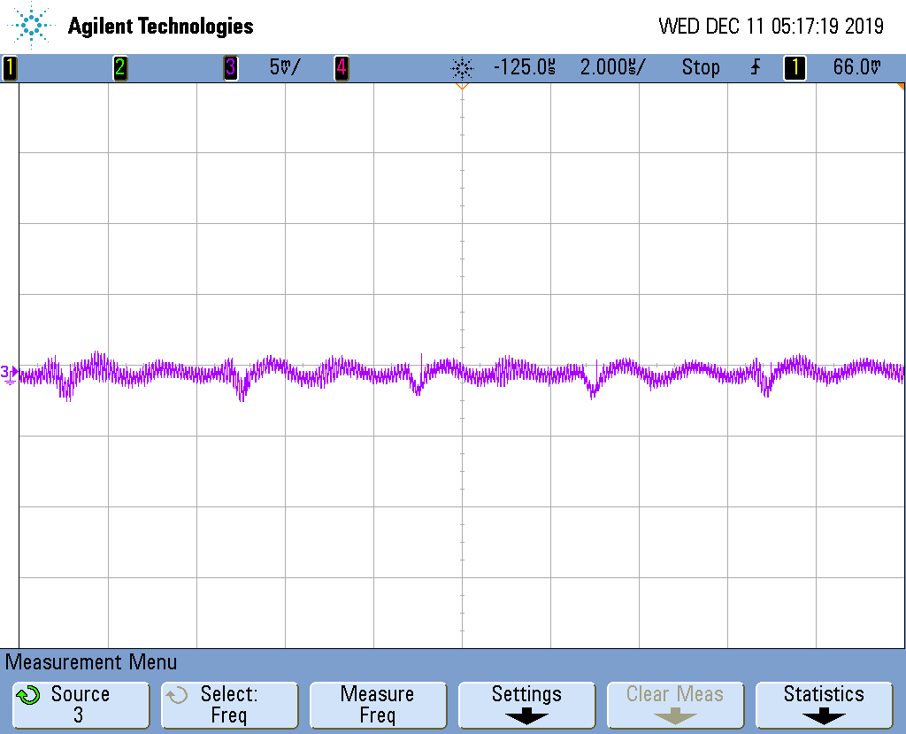
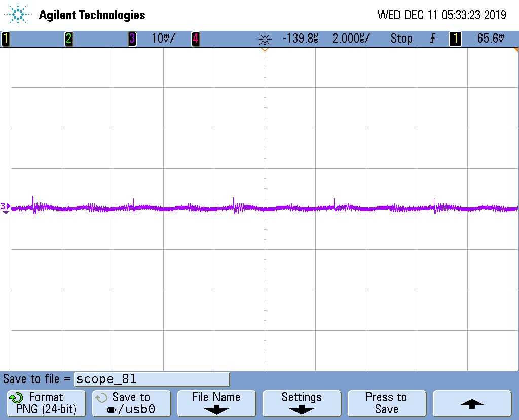
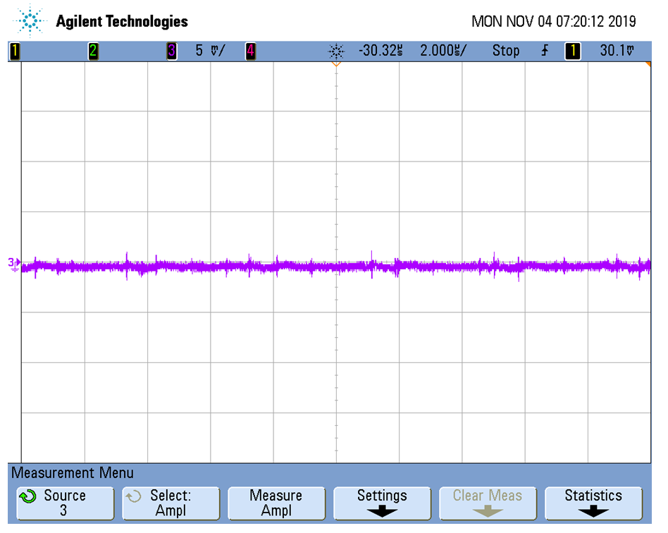
Figure 3-3 and Figure 3-5 shows the output ripple of the high voltage circuit of both negative and positive rail at full load, respectively. The ripple is measured at the output capacitor before the π filter, the peak to peak ripple is close to 25 mV. Figure 3-4 and Figure 3-6 shows the ripple measured after the Power Filter, which is significantly attenuated.
 Figure 3-3 Output Ripple of Negative
Rail Before Power Filter
 Figure 3-5 Output Ripple of Positive
Rail Before Power Filter
 Figure 3-4 Output Ripple of Negative
Rail After Power Filter
 Figure 3-6 Output Ripple of Positive
Rail After Power Filter