SLOS154C December 1995 – July 2025 TLC27L1 , TLC27L1A , TLC27L1B
PRODUCTION DATA
- 1
- 1 Features
- 2 Applications
- 3 Description
- 4 Pin Configuration and Functions
-
5 Specifications
- 5.1 Absolute Maximum Ratings
- 5.2 Dissipation Ratings
- 5.3 Recommended Operating Conditions
- 5.4 Electrical Characteristics, C Suffix
- 5.5 Operating Characteristics, VDD = 5V, C Suffix
- 5.6 Operating Characteristics, VDD = 10V, C Suffix
- 5.7 Electrical Characteristics, I Suffix
- 5.8 Operating Characteristics, VDD = 5V, I Suffix
- 5.9 Operating Characteristics, VDD = 10V, I Suffix
- 5.10 Typical Characteristics
- 6 Parameter Measurement Information
- 7 Application and Implementation
- 8 Device and Documentation Support
- 9 Revision History
- 10Mechanical, Packaging, and Orderable Information
5.10 Typical Characteristics
data at high and low temperatures applicable only within rated operating free-air temperature ranges of the various devices
Table of Graphs
| TYPICAL CHARACTERISTIC | FIGURE | ||
|---|---|---|---|
| VIO | Input offset voltage | Distribution | Figure 5-1, Figure 5-2 |
| αVIO | Temperature coefficient | Distribution | Figure 5-3, Figure 5-4 |
| VOH | High-level output voltage | vs High-level output current | Figure 5-5, Figure 5-6 |
| vs Supply voltage | Figure 5-7 | ||
| vs Free-air temperature | Figure 5-8 | ||
| VOL | Low-level output voltage | vs Common-mode input voltage | Figure 5-9, Figure 5-10 |
| vs Differential input voltage | Figure 5-11 | ||
| vs Free-air temperature | Figure 5-12 | ||
| vs Low-level output current | Figure 5-13, Figure 5-14 | ||
| AVD | Large-signal differential voltage amplification | vs Supply voltage | Figure 5-15 |
| vs Free-air temperature | Figure 5-16 | ||
| vs Frequency | Figure 5-25, Figure 5-26 | ||
| IIB | Input bias current | vs Free-air temperature | Figure 5-17 |
| IIO | Input offset current | vs Free-air temperature | Figure 5-17 |
| VI | Maximum input voltage | vs Supply voltage | Figure 5-18 |
| IDD | Supply current | vs Supply voltage | Figure 5-19 |
| vs Free-air temperature | Figure 5-20 | ||
| SR | Slew rate | vs Supply voltage | Figure 5-21 |
| vs Free-air temperature | Figure 5-22 | ||
| Bias-select current | vs Supply voltage | Figure 5-23 | |
| VO(PP) | Maximum peak-to-peak output voltage | vs Frequency | Figure 5-24 |
| φm | Phase margin | vs Supply voltage | Figure 5-27 |
| vs Free-air temperature | Figure 5-28 | ||
| vs Capacitive load | Figure 5-29 | ||
| Vn | Equivalent input noise voltage | vs Frequency | Figure 5-30 |
| Phase shift | vs Frequency | Figure 5-25, Figure 5-26 | |
 Figure 5-1 Distribution of TLC27L1
Input Offset Voltage
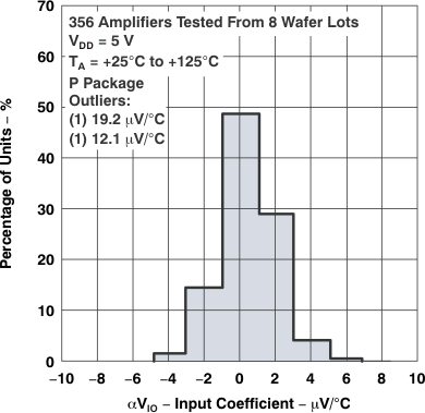 Figure 5-3 Distribution of TLC27L1
Input Offset Voltage
Temperature Coefficient
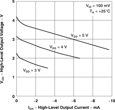 Figure 5-5 High-Level Output Voltage
vs
High-Level Output Current
 Figure 5-7 High-Level Output Voltage
vs
Supply Voltage
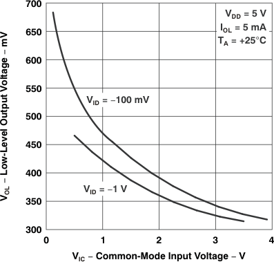 Figure 5-9 Low-Level Output Voltage
vs
Common-Mode Input Voltage
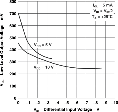 Figure 5-11 Low-Level Output Voltage
vs
Differential Input Voltage
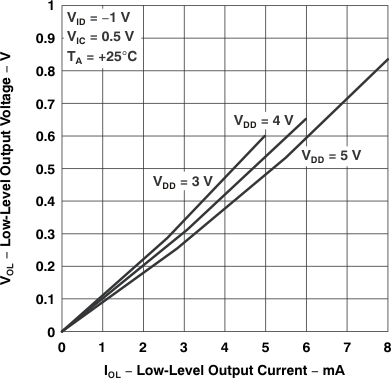 Figure 5-13 Low-Level Output Voltage
vs
Low-Level Output Current
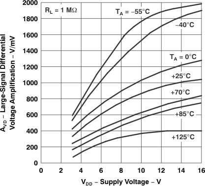 Figure 5-15 Large-Signal
 differential Voltage Amplification
vs Supply Voltage
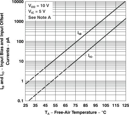
| Typical values of input bias current and input offset current less than 5pA determined mathematically |
vs
Free-Air Temperature
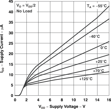 Figure 5-19 Supply Current
vs
Supply Voltage
 Figure 5-21 Slew Rate
vs
Supply Voltage
 Figure 5-23 Bias-Select Current
vs
Supply Voltage
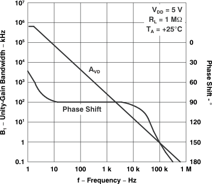 Figure 5-25 Large-Signal Differential
Voltage
Figure 5-25 Large-Signal Differential
VoltageAmplification and Phase Shift
vs Frequency
 Figure 5-27 Phase Margin
vs
Supply Voltage
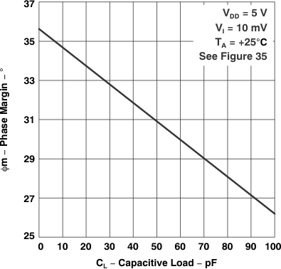 Figure 5-29 Phase Margin
vs
Capacitive Load
 Figure 5-2 Distribution of TLC27L1
Input Offset Voltage
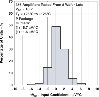 Figure 5-4 Distribution of TLC27L1
Input Offset Voltage
Temperature Coefficient
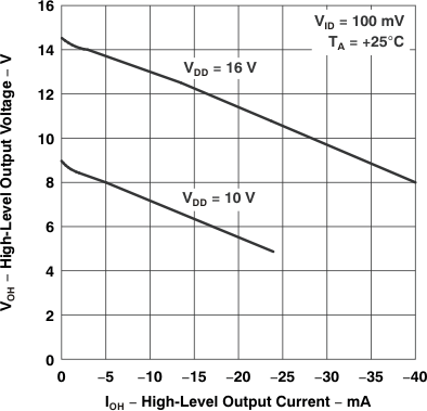 Figure 5-6 High-Level Output Voltage
vs
High-Level Output Current
 Figure 5-8 High-Level Output Voltage
vs
Free-Air Temperature
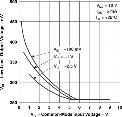 Figure 5-10 Low-Level Output Voltage
vs
Common-Mode Input Voltage
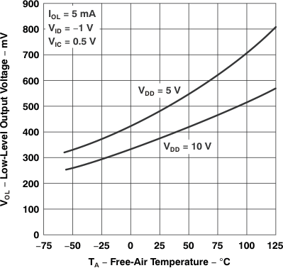 Figure 5-12 Low-Level Output Voltage
vs
Free-Air Temperature
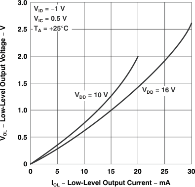 Figure 5-14 Low-Level Output Voltage
vs
Low-Level Output Current
 Figure 5-16 Large-Signal
 Differential Voltage Amplification
vs Free-Air Temperature
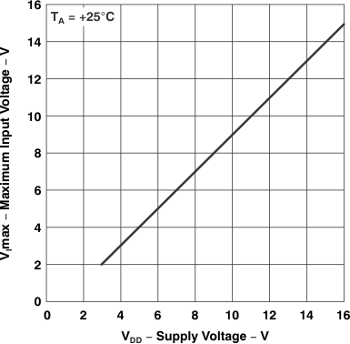
vs
Supply Voltage
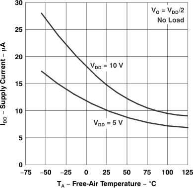 Figure 5-20 Supply Current
vs
Free-Air Temperature
 Figure 5-22 Slew Rate
vs
Free-Air Temperature
 Figure 5-24 Maximum Peak-to-Peak
Output Voltage
Figure 5-24 Maximum Peak-to-Peak
Output Voltagevs
Frequency
 Figure 5-26 Large-Signal Differential
Voltage
Figure 5-26 Large-Signal Differential
VoltageAmplification and Phase Shift
vs Frequency
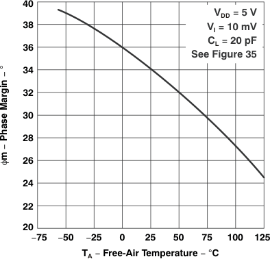 Figure 5-28 Phase Margin
vs
Free-Air Temperature
 Figure 5-30 Equivalent Input Noise
Voltage
Figure 5-30 Equivalent Input Noise
Voltagevs
Frequency