SLUA963B June 2020 – October 2022 UCC21710-Q1 , UCC21732-Q1 , UCC5870-Q1
- HEV/EV Traction Inverter Design Guide Using Isolated IGBT and SiC Gate Drivers
- 1Introduction
- 2HEV/EV Overview
-
3Design of HEV/EV Traction Inverter Drive Stage
- 3.1 Introduction to UCC217xx-Q1
- 3.2 Designing a Traction Inverter Drive System Using UCC217xx-Q1
- 3.3 Description of Protection Features
- 3.4 Protection Features of UCC217xx-Q1
- 3.5
UCC217xx-Q1 Protection and Monitoring Features Descriptions
- 3.5.1 Primary and Secondary Side UVLO and OVLO
- 3.5.2 Over-Current (OC) and Desaturation (DESAT) Detection
- 3.5.3 2-Level and Soft Turn-Off
- 3.5.4 Power Switch Gate Voltage (VGE/VGS) Monitoring
- 3.5.5 Power Switch Anti-Shoot-Through
- 3.5.6 Integrated Internal or External Miller Clamp
- 3.5.7 Isolated Analog-to-PWM Channel
- 3.5.8 Short-Circuit Clamping
- 3.5.9 Active Pulldown
- 3.6 Introduction to UCC5870-Q1
- 3.7 Designing a Traction Inverter Drive System Using UCC5870-Q1
- 3.8 Description of Protection Features
- 3.9 Protection Features of UCC5870-Q1
- 3.10
UCC5870-Q1 Protection and Monitoring Features Descriptions
- 3.10.1 Primary and Secondary Side UVLO and OVLO
- 3.10.2 Programmable Desaturation (DESAT) Detection and Over-Current (OC)
- 3.10.3 Adjustable 2-Level or Soft Turn-Off
- 3.10.4 Active High-Voltage Clamp
- 3.10.5 Power Switch Gate Voltage (VGE/VGS) Monitoring
- 3.10.6 Gate Threshold Voltage Monitor
- 3.10.7 Power Switch Anti-Shoot-Through
- 3.10.8 Active Short Circuit (ASC)
- 3.10.9 Integrated Internal or External Miller Clamp
- 3.10.10 Isolated Analog-to-Digital Converter
- 3.10.11 Short-Circuit Clamping
- 3.10.12 Active and Passive Pulldown
- 3.10.13 Thermal Shutdown and Temperature Warning of Driver IC
- 3.10.14 Clock Monitor and CRC
- 3.10.15 SPI and Register Data Protection
- 4Isolated Bias Supply Architecture
- 5Summary
- 6References
- 7Revision History
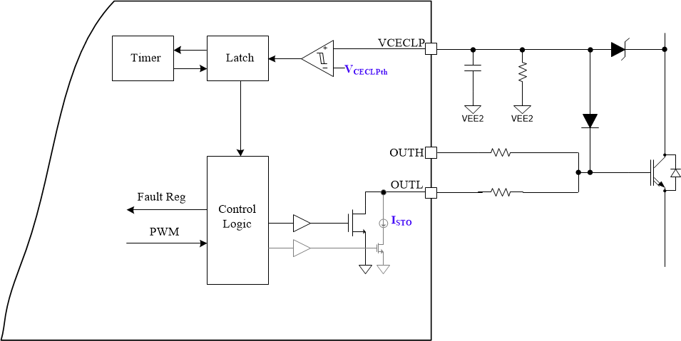
3.10.4 Active High-Voltage Clamp
The active high voltage clamping feature protects power transistors from over-voltage damage during switching transitions, specifically turn-off, while reducing the power dissipated in the external TVS clamp diodes used to protect the power FET. The UCC5870-Q1 has a designated input pin, VCECLP, that monitors the voltage during turn-off. When the VCE of the FET increases enough to turn on the external TVS diode, the RC network at the VCECLP input is charged up. Once the voltage at VCECLP reaches the clamp threshold (VCECLPTH), OUTL drive strength changes from the normal pull-down strength (can be >15A) to the ISTO (soft turn-off) setting in order to slow down the turn-off and reduce the voltage overshoot. The high-voltage clamping remains active for a predefined time tVCECLP_HLD. The OV condition is reported to a Status Register and, if unmasked, nFLT1 pulls low. The circuit implementation is shown in Figure 3-19.
 Figure 3-19 Integrated active high-voltage clamping configuration