SLUAA84A January 2021 – February 2022 BQ769142 , BQ76942 , BQ76952
1 Introduction
The BQ769x2 family of battery monitor devices is designed with integrated high-side N-channel MOSFET drivers CHG and DSG. High-side switching allows easy interface to the battery with simple communication interfaces referenced to PACK- which can still operate when the battery is protected. The data sheet and evaluation module schematics and Figure 1-1 show FETs on the high-side current path. The BQ769x2 uses series FETs connected in a common drain configuration. The charge FET pulls the charger down to the battery voltage when on and the discharge FET pulls the load up to PACK+ when on. Low-side switching may be desired when the system specifications include an isolated interface, or require low side switching, or the design implements FETs not easily driven on the high side. Figure 1-2 shows FETs on the low side, again with a common drain configuration. The discharge FET pulls PACK- down to battery negative when on and the charge FET pulls the charger negative up to the battery negative voltage when on.
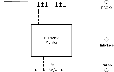 Figure 1-1 High-Side
FETs
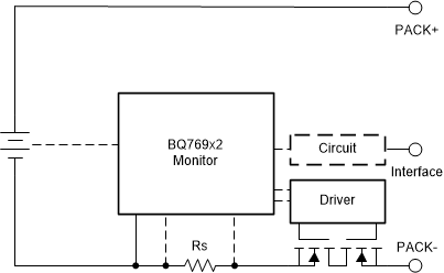 Figure 1-2 Low-Side
FETs
Figure 1-2 Low-Side
FETsThe BQ769x2 does not include integrated low-side drivers, but has digital outputs DDSG and DCHG which combine the FET output states with the precharge and predischarge states and can signal the desired state of the FETs. To implement a driver it is good to look at the voltage range needed for the FET gates. With the circuit "GND" reference at the battery negative, when the discharge FET is off the discharge FET gate is at GND and PACK- can be pulled to the PACK+ by a load resistance as shown in Figure 1-3. The system cannot charge in this state and the charge FET can be off with the gate voltage at VBAT also. When the discharge FET is turned on its gate voltage is raised to a voltage VFETON which will turn on the discharge FET. PACK- is pulled down toward the GND voltage as shown in Figure 1-4. The charge FET gate can also be turned on by the VFETON voltage to eliminate the voltage drop across the body diode and avoid heating the FET. Neglecting the voltage drop of the sense resistor and FET resistances PACK- voltage is at GND.
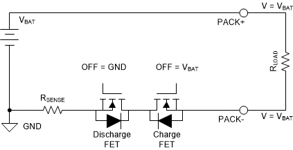 Figure 1-3 Discharge FET Off, Load
Attached
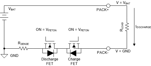 Figure 1-4 Discharge FET On, Load
Attached
Figure 1-4 Discharge FET On, Load
AttachedWhen the charge FET is off with a charger attached, the PACK- voltage is pushed below the GND level. For the charge FET to stay off the gate voltage must be near the PACK- voltage as shown in Figure 1-5. When the charge FET is on with the charger attached, the gate is raised to the VFETON voltage and PACK- is pulled up toward GND, see Figure 1-6.
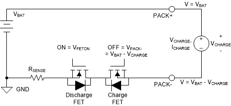 Figure 1-5 Charge FET Off,
Charger Attached
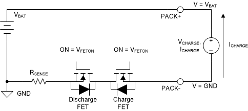 Figure 1-6 Charge FET On,
Charger Attached
Figure 1-6 Charge FET On,
Charger AttachedIf a reversed charger can be connected to the battery both the battery and charger want to push current in the same direction. Once the fault is detected and the FETs open, the reversed charger pushes the PACK- voltage above the PACK+ voltage. The discharge FET must withstand the high voltage, and the charge FET gate voltage must rise to prevent damage to the FET. This condition is shown in Figure 1-7.
Figure 1-8 summarizes the voltage range of the FET gates. The discharge gate must move from VFETON when on to GND when off. The charge FET gate voltage must move from VFETON to the PACK- voltage to turn the FET off, but depending on the FET and system conditions that voltage may have a large range above or below the battery voltage. A driver circuit design will need to provide and accommodate these voltage ranges.
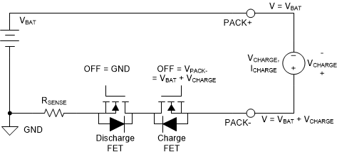 Figure 1-7 Reversed
Charger, FETs Off
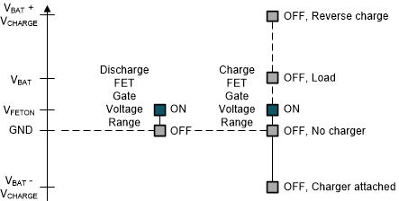 Figure 1-8 Voltage Range
for Low Side FET Gates