SLUAA84A January 2021 – February 2022 BQ769142 , BQ76942 , BQ76952
5 FET Driver Implementation
An IC FET driver will provide the level shift from logic level signals to an appropriate gate drive level with a suitable output stage. The implementation in Figure 5-1 uses the UCC27524 dual noninverting FET driver. One driver is used for turn on and off of the discharge FET, the other for turn on of the charge FET. Turn off of the charge FET is provided by RGS or a circuit on the gate. The UCC27524 is a very capable driver designed to switch gates very quickly in switching regulator or other applications. Here as a load switch a series resistor will be needed to slow gate switching to avoid a large inductive response during turn off of a high current event such as overcurrent or short circuit protection. U2 is a linear regulator used in this test, it is blocked from discharging during a battery short circuit by D12, and the input is filtered with R68 and its input capacitors. Another suitable source could be used if available in an application. A circuit with four discharge and charge FETs is shown in Figure 5-2. The circuit configuration is much like the logic level FET circuit but the diode D3 is a conventional diode since there is more voltage available from the driver. Test circuits in this application report with high voltage drive options use CSD19536KCS FETs.
Figure 5-3 and Figure 5-4 show the very capable response of the driver, and the discharge FET switching without D6 and R28 in Figure 5-2. The gate voltage is slowed by the R-C response of the series resistor to the gates and the gate capacitance. Since the threshold voltage of the FETs is closer to GND than to the drive level note the delay between the DSGDRV signal fall and the current transition. Adding D6 and R28 does not change the turn on which is shown in more detail in Figure 5-5, but speeds up the turn off as shown in Figure 5-6. The R28 value may be adjusted for faster turn off. Switching of the charge FETs is shown in Figure 5-7 and Figure 5-8.
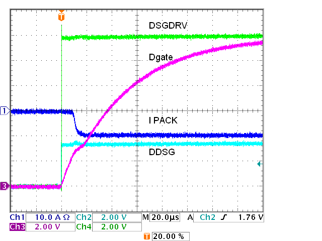 Figure 5-3 IC
FET Driver, Four Discharge FETs, On
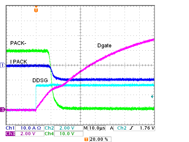 Figure 5-5 IC FET Driver, Four
Discharge FETs, Schottky, On
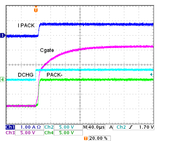 Figure 5-7 IC
FET Driver, Four Charge FETs, On
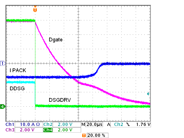 Figure 5-4 IC
FET Driver, Four Discharge FETs, Off
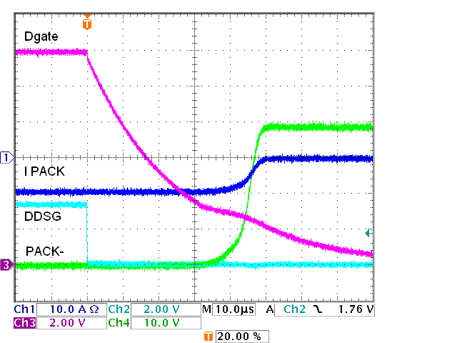 Figure 5-6 IC FET Driver, Four
Discharge FETs, Schottky, Off
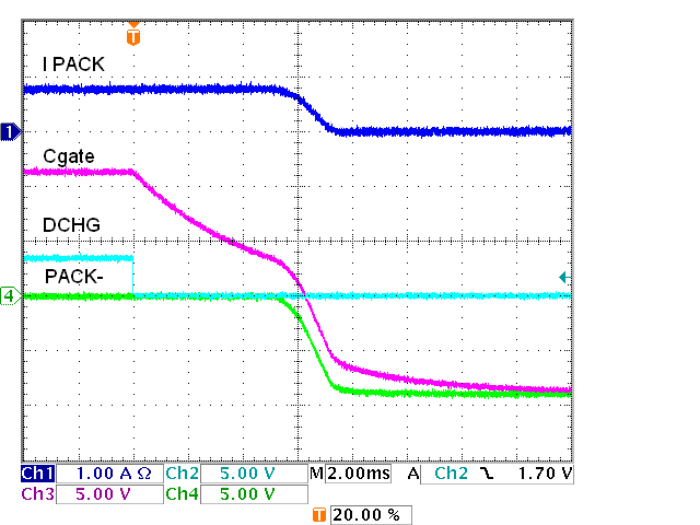 Figure 5-8 IC
FET Driver, Four Charge FETs, Off, 91 kΩ
Figure 5-8 IC
FET Driver, Four Charge FETs, Off, 91 kΩAn implementation with 12 discharge and charge FETs is shown in Figure 5-9. With 12 FETs the total capacitance of the gates is larger. For DSG a smaller resistor is used. The individual gate resistors such as R29 are no longer a small part of the total resistance to the gate, so it may be more appropriate to replace these with ferrite beads, however testing used the 51-Ω resistors. In the charge path the PNP transistor is added to aid in turn off to avoid a small resistor which would be biased while CHG is on. Results are shown in Figure 5-10 and the following figures. Notice that with the PNP turn off circuit even though there are more FETs the charge FETs are off earlier in Figure 5-13 than with the pulldown resistor only in Figure 5-8. Turn off could be adjusted with the R24 base resistor value.
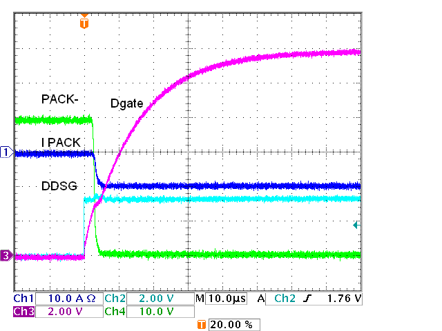 Figure 5-10 IC FET Driver, 12 Discharge
FETs, On
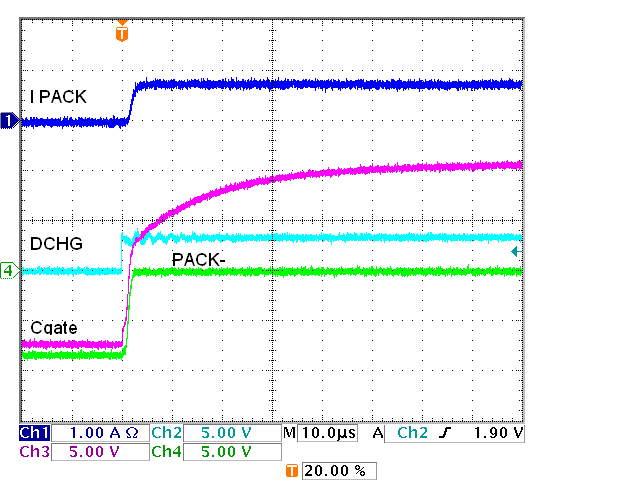 Figure 5-12 IC FET Driver, 12 Charge
FETs, On
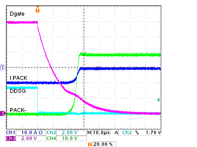 Figure 5-11 IC FET Driver, 12 Discharge
FETs, Off
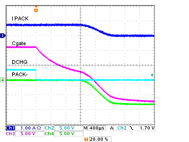 Figure 5-13 IC FET Driver, 12 Charge
FETs, Off
Figure 5-13 IC FET Driver, 12 Charge
FETs, OffWhen switching multiple FETs it is important to check the supply during the switching. Figure 5-14 shows the 12-V regulator output when the 24 FETs are turned on. The current pulls down the regulator input which is made up over time. The regulator has sufficient headroom so that the dip is not significant, the regulated voltage remains constant.
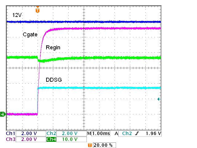 Figure 5-14 12-V Power When 24 FETs Switch
On