SLUAA84A January 2021 – February 2022 BQ769142 , BQ76942 , BQ76952
4 Logic Level FETs
Some designers will recognize that REG1 can be set to 5 V and may want to consider the use of logic level FETs controlled directly by the DDSG and DCHG outputs. DDSG and DDCHG provide the switching function and 5 V as the VFETON level. Test conditions for the digital outputs show VOH and VOL with 5-mA source or sink current which is encouraging, but the test condition load is 10 pF and no rise or fall time is specified.
Data memory configuration would change for REG1 at 5 V.
Settings:Configuration:REG12 Config 0x0F
While a designer might buffer the signals with a more capable 5-V driver, this application report shows examples of direct drive of the FETs with the digital outputs. CSD18535KCS FETs are used which have a RDSON specification at 4.5 V. Figure 4-1 shows an example schematic for driving FETs with the DDSG and DCHG signals. The 51-Ω resistors are used to isolate the gates from each other when using parallel FETs to avoid high frequency oscillation. With a single FET the 51-Ω resistors were retained in this test circuit and add to the drive resistance.
When driving a single discharge FET with a 1-kΩ gate resistance R27, ringing of the driver was observed in Figure 4-2. This is an effect of the FET used, the trace parasitics, and the inability of the driver to maintain a suitable drive current for the FET. With four FETs the additional load on the driver from the additional Ciss slows the turn on and avoids the ringing. Figure 4-3 shows however that the load pulls down the regulator voltage temporarily. If this is undesired the capacitor on REG1 can be increased. The test waveforms in this section do not include an increased REG1 capacitance.
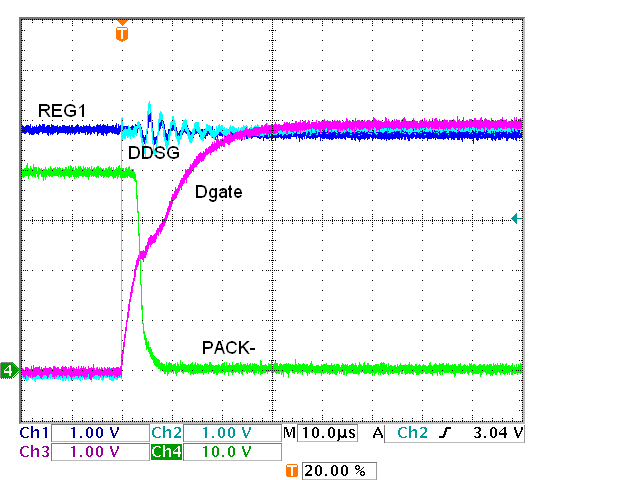 Figure 4-2 Discharge FET Turn On with One FET, 1-kΩ Gate
Resistance
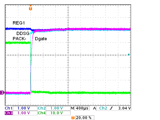 Figure 4-3 Discharge FET Turn On with Four FETs, 1 kΩ,
REG1 Droop
Figure 4-3 Discharge FET Turn On with Four FETs, 1 kΩ,
REG1 DroopWith the board topology established, the adjustment available to the designer to avoid gate ringing is the gate resistor R27. Increasing the resistance slows the FET turn on and avoids the ringing. A 3-kΩ value was selected, turn on and turn off with a single FET is shown in Figure 4-4 and Figure 4-5.
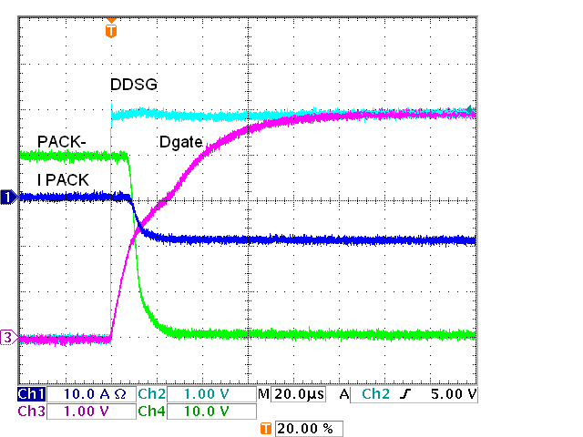 Figure 4-4 DDSG Drive, One FET, On,
3-kΩ Gate Resistor
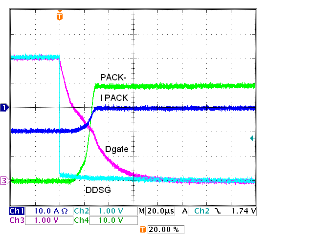 Figure 4-5 DDSG Drive, One FET, Off,
3-kΩ Gate Resistor
Figure 4-5 DDSG Drive, One FET, Off,
3-kΩ Gate ResistorWhen the charge FET is off, the charger is free to pull the PACK- terminal below the battery negative which is GND. When DCHG goes high the charge FET will turn on. Voltage swing is small in this case and driver ringing was not observed in this test. An example of single charge FET turn on using a 1-kΩ gate resistor is shown in Figure 4-6. Turn off is shown in Figure 4-7. Note that DCHG goes low quickly since it does not drive the gate, current is blocked to the driver by D3. The gate-source resistor R35 turns off the FET, in this test it is 1 MΩ so turn off is slow. Also notice that the 10M scope probe pulls up on the Cgate signal creating a voltage divider and holding the gate slightly above the PACK- signal.
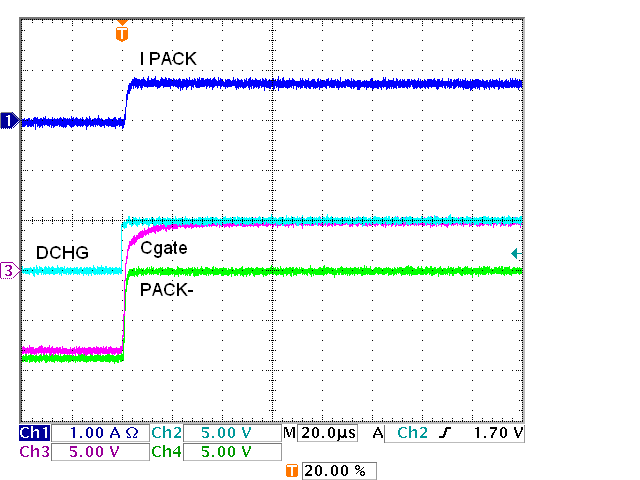 Figure 4-6 DCHG Drive, One FET,
On
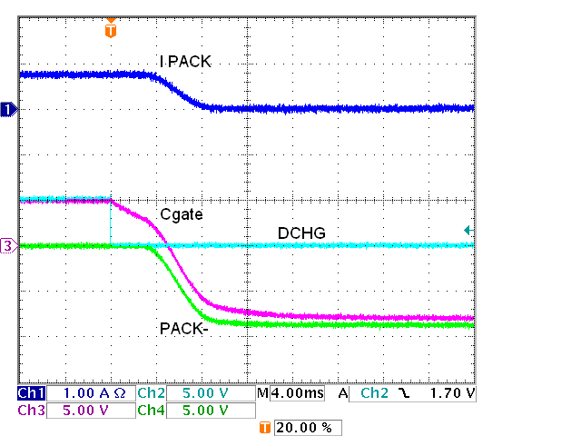 Figure 4-7 DCHG Drive, One FET,
Off
Figure 4-7 DCHG Drive, One FET,
OffFigure 4-8 shows a schematic with four FETs. With the larger combined gate capacitance a 1-kΩ resistor is used for R27. Since a slow turn off is undesired for discharge due to the higher discharge currents expected, a Schottky diode is used to provide a parallel resistance path with R28 for turn off . The diode D6 blocks current to the gates during turn on but allows the DDSG to pull current from the gates through both R27 and R28 during turn off.
With four FETs and a 1-kΩ drive resistance the DDSG does not ring in this test. A droop can be seen in the DDSG in Figure 4-9 as the FETs come on. Figure 4-10 shows turn off with the added D6 Schottky and R28 1-kΩ path of Figure 4-8. R28 could be made smaller for faster turn off , or a PNP transistor circuit would require only control current from DDSG.
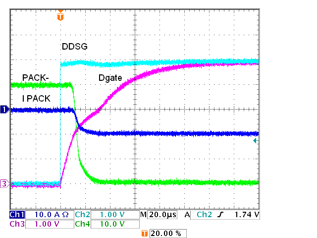 Figure 4-9 DDSG Drive, Four FETs, On, 1 kΩ,
Schottky
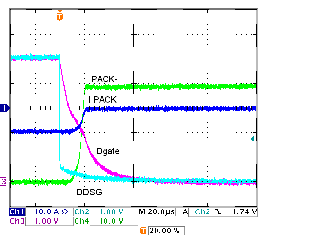 Figure 4-10 DDSG Drive, Four FETs, Off, 1 kΩ,
Schottky
Figure 4-10 DDSG Drive, Four FETs, Off, 1 kΩ,
SchottkyTurning on CHG with four FETs is shown in Figure 4-11. Turning off the four FETs accomplished by the 1-MΩ RGS is shown in Figure 4-12. Turn off is slow due to that large resistance used to limit current while the FET is on.
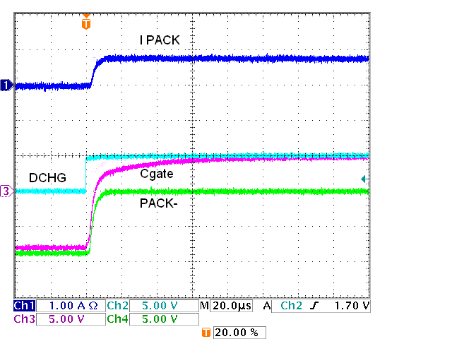 Figure 4-11 DCHG Drive, Four FETs, On, 1 kΩ, 1-MΩ
RGS
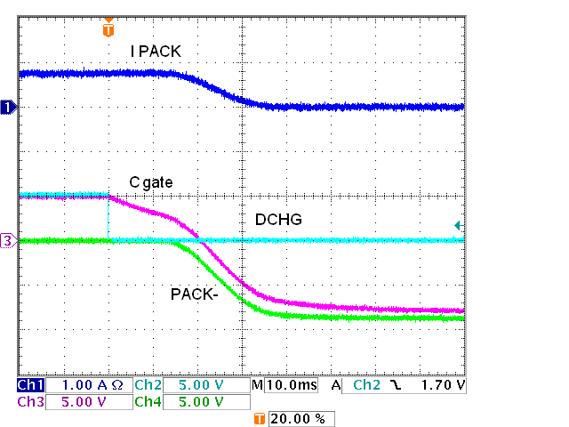 Figure 4-12 DCHG Drive, Four FETs, Off, 1 kΩ, 1-MΩ
RGS
Figure 4-12 DCHG Drive, Four FETs, Off, 1 kΩ, 1-MΩ
RGSWhen faster turn off is desired, there is little voltage margin for circuits with the REG1 voltage and logic level FETs. One solution is to use a smaller RGS resistor R35. Using a 91-kΩ RGS is shown in Figure 4-13 and Figure 4-14. Turn on is similar to the larger RGS waveform, while turn off is much faster. With the 5-V supply this solution requires approximately 50 μA additional current while the charge FET is on.
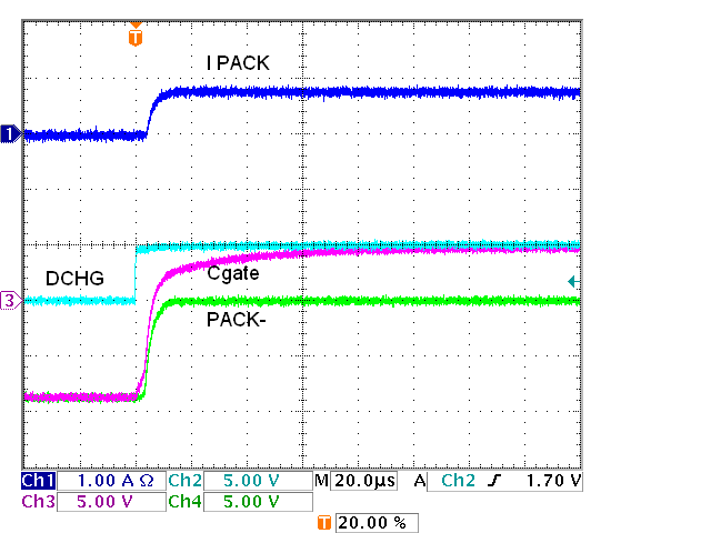 Figure 4-13 DCHG Drive, Four FETs, On, 91-kΩ
RGS
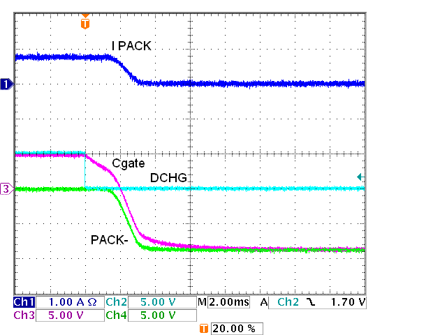 Figure 4-14 DCHG Drive, Four FETs, Off, 91-kΩ
RGS
Figure 4-14 DCHG Drive, Four FETs, Off, 91-kΩ
RGSWhen considering a logic level FET solution a designer should perform a tolerance analysis. With the tolerance on REG1 and the Schottky diode at D3, a sufficiently low RGSON FET should be used.