SLUAA84A January 2021 – February 2022 BQ769142 , BQ76942 , BQ76952
2 Circuit Concepts
A FET driver circuit then will need to take the digital control signal from the BQ769x2, provide a supply voltage for the VFETON high level, and provide for switching the gates accommodating the voltage range in Figure 1-8 with a speed suitable for the system design.
Figure 2-1 shows a basic circuit approach where a regulator provides a VFETON voltage for a driver which provides level shifting of the digital signal from the BQ76952 to the VFETON voltage. The resistor R4 brings the drive voltage to the discharge FET gate. With the extra range of the charge FET gate, Q3 allows the gate voltage to go negative when the Cdrive is off. D1 blocks current into the driver when PACK- is high. D2 limits the gate -source voltage of the Q1 charge FET. R1 provides a current limit from the driver as Cdrive turns on if Q1 is slow to turn on. R2 turns off the FET when Cdrive goes low since D1 prevents the driver from pulling current from the gate.
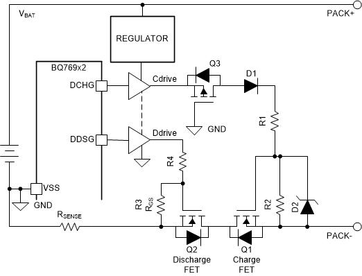 Figure 2-1 Simple Driver Circuit,
Resistive Charge Turn Off
Figure 2-1 Simple Driver Circuit,
Resistive Charge Turn OffWhen the driver can accept its output being pulled above the supply, a circuit such as Figure 2-2 might be used. D3 limits the voltage to the driver to its safe level and the gate-source voltage of Q3. R1 provides a limited current bypass past D1 so that the driver can help pull down the gate; it must limit the current back into D3 when PACK- is at its maximum voltage. So turn off will still be slow, and once Q1 begins to turn off and PACK- falls, it is R2 which completes turn off of the charge FET Q1. Since most IC drivers have an ABS MAX output of the driver voltage, a special driver is required for this type implementation.
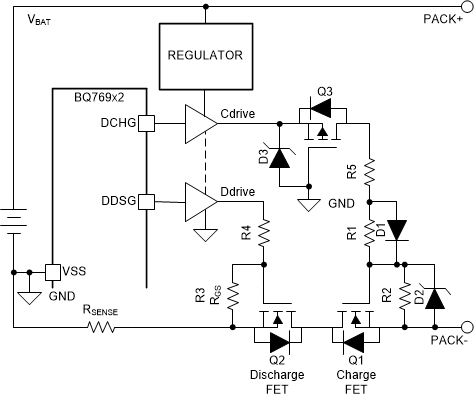 Figure 2-2 Driver with Limited Turn Off Current
Figure 2-3 shows a concept where the charge FET Q1 is driven on by the driver or is clamped off by Q4. This technique could be very effective at turning off Q1, but would require continuous current whether the charge FET was on or off.
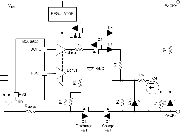 Figure 2-3 Driver with Charge FET Driven Clamp
Figure 2-4 is much like the simple driver circuit but with a gain circuit to help turn off the charge FET more quickly than with R2 alone. This circuit is powered by the Q1 gate voltage and Q4 will be on while voltage is present even as PACK- drops below GND. Either a PNP or P-channel FET could be used for Q4, the FET would be voltage controlled requiring less current, but VGSth may be larger than the VBE of the PNP transistor. The additional diode D3 keeps the base of Q4 above the emitter when the driver is on. The driver must provide current for both the RGS resistor R2 and the base resistor R5, so more current is required than the simple driver circuit while the FET is on.
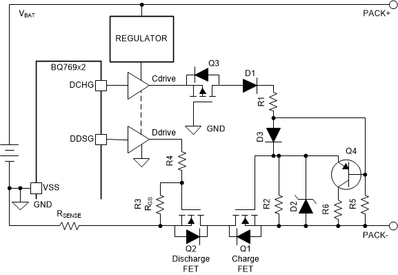 Figure 2-4 Charge FET Driver with PNP Turn Off
A high performance option would be to use an isolated gate driver for the charge path as represented in Figure 2-5. The isolated driver would be very effective at driving the charge FET gate high or low as needed regardless of the PACK- voltage, but would require an isolated power supply.
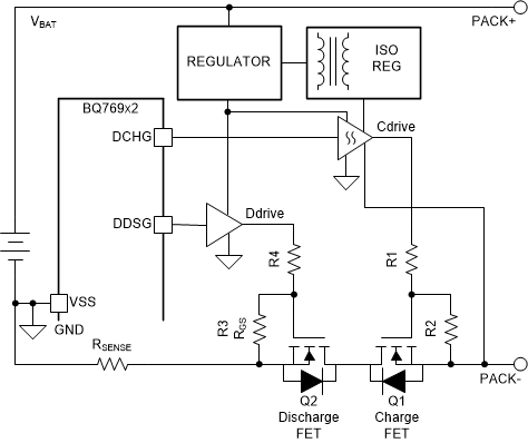 Figure 2-5 Isolated Driver
Test circuits in this application report use the simple driver concept of Figure 2-1 and the PNP circuit of Figure 2-4.