SLUSCD1C June 2017 – November 2018 TPS2373
PRODUCTION DATA.
- 1 Features
- 2 Applications
- 3 Description
- 4 Revision History
- 5 Pin Configuration and Functions
- 6 Specifications
-
7 Detailed Description
- 7.1 Overview
- 7.2 Functional Block Diagram
- 7.3
Feature Description
- 7.3.1 APD Auxiliary Power Detect
- 7.3.2 PG Power Good (Converter Enable) Pin Interface
- 7.3.3 CLSA and CLSB Classification
- 7.3.4 DEN Detection and Enable
- 7.3.5 Internal Pass MOSFET
- 7.3.6 TPH, TPL and BT PSE Type Indicators
- 7.3.7 VC_IN, VC_OUT, UVLO_SEL, and Advanced PWM Startup
- 7.3.8 AMPS_CTL, MPS_DUTY and Automatic MPS
- 7.3.9 VDD Supply Voltage
- 7.3.10 VSS
- 7.3.11 Exposed Thermal PAD
- 7.4
Device Functional Modes
- 7.4.1 PoE Overview
- 7.4.2 Threshold Voltages
- 7.4.3 PoE Startup Sequence
- 7.4.4 Detection
- 7.4.5 Hardware Classification
- 7.4.6 Inrush and Startup
- 7.4.7 Maintain Power Signature
- 7.4.8 Advanced Startup and Converter Operation
- 7.4.9 PD Hotswap Operation
- 7.4.10 Startup and Power Management, PG and TPH, TPL, BT
- 7.4.11 Adapter ORing
- 7.4.12 Using DEN to Disable PoE
- 7.4.13 ORing Challenges
-
8 Application and Implementation
- 8.1 Application Information
- 8.2
Typical Application
- 8.2.1 Design Requirements
- 8.2.2
Detailed Design Requirements
- 8.2.2.1 Input Bridges and Schottky Diodes
- 8.2.2.2 Protection, D1
- 8.2.2.3 Capacitor, C1
- 8.2.2.4 Detection Resistor, RDEN
- 8.2.2.5 Classification Resistors, RCLSA and RCLSB
- 8.2.2.6 APD Pin Divider Network RAPD1, RAPD2
- 8.2.2.7 Opto-isolators for TPH, TPL and BT
- 8.2.2.8 VC Input and Output, CVCIN and CVCOUT
- 8.2.2.9 UVLO Select, UVLO_SEL
- 8.2.2.10 Automatic MPS and MPS Duty Cycle, RMPS and RMPS_DUTY
- 8.2.2.11 Internal Voltage Reference, RREF
- 8.2.3 Application Curves
- 9 Power Supply Recommendations
- 10Layout
- 11Device and Documentation Support
- 12Mechanical, Packaging, and Orderable Information
7.4.11 Adapter ORing
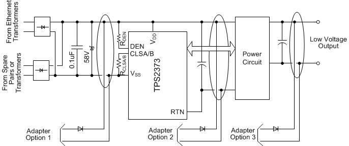
Many PoE-capable devices are designed to operate from either a wall adapter or PoE power. A local power solution adds cost and complexity, but allows a product to be used if PoE is not available in a particular installation. While most applications only require that the PD operate when both sources are present, the TPS2373 supports forced operation from either of the power sources. Figure 29 illustrates three options for diode ORing external power into a PD. Only one option would be used in any particular design. Option 1 applies power to the TPS2373 PoE input, option 2 applies power between the TPS2373 PoE section and the power circuit, and option 3 applies power to the output side of the converter. Each of these options has advantages and disadvantages. Many of the basic ORing configurations and much of the discussion contained in the application note Advanced Adapter ORing Solutions using the TPS23753 (SLVA306), apply to the TPS2373 incorporating a DC/DC converter.
 Figure 29. Oring Configurations
 The IEEE standards require that the Ethernet cable be isolated from ground and all other system potentials. The adapter must meet a minimum 1500 Vac dielectric withstand test between the output and all other connections for ORing options 1 and 2. The adapter only needs this isolation for option 3 if it is not provided by the converter.
Adapter ORing diodes are shown for all the options to protect against a reverse voltage adapter, a short on the adapter input pins, or damage to a low-voltage adapter. ORing is sometimes accomplished with a MOSFET in option 3.