SLUSCD1C June 2017 – November 2018 TPS2373
PRODUCTION DATA.
- 1 Features
- 2 Applications
- 3 Description
- 4 Revision History
- 5 Pin Configuration and Functions
- 6 Specifications
-
7 Detailed Description
- 7.1 Overview
- 7.2 Functional Block Diagram
- 7.3
Feature Description
- 7.3.1 APD Auxiliary Power Detect
- 7.3.2 PG Power Good (Converter Enable) Pin Interface
- 7.3.3 CLSA and CLSB Classification
- 7.3.4 DEN Detection and Enable
- 7.3.5 Internal Pass MOSFET
- 7.3.6 TPH, TPL and BT PSE Type Indicators
- 7.3.7 VC_IN, VC_OUT, UVLO_SEL, and Advanced PWM Startup
- 7.3.8 AMPS_CTL, MPS_DUTY and Automatic MPS
- 7.3.9 VDD Supply Voltage
- 7.3.10 VSS
- 7.3.11 Exposed Thermal PAD
- 7.4
Device Functional Modes
- 7.4.1 PoE Overview
- 7.4.2 Threshold Voltages
- 7.4.3 PoE Startup Sequence
- 7.4.4 Detection
- 7.4.5 Hardware Classification
- 7.4.6 Inrush and Startup
- 7.4.7 Maintain Power Signature
- 7.4.8 Advanced Startup and Converter Operation
- 7.4.9 PD Hotswap Operation
- 7.4.10 Startup and Power Management, PG and TPH, TPL, BT
- 7.4.11 Adapter ORing
- 7.4.12 Using DEN to Disable PoE
- 7.4.13 ORing Challenges
-
8 Application and Implementation
- 8.1 Application Information
- 8.2
Typical Application
- 8.2.1 Design Requirements
- 8.2.2
Detailed Design Requirements
- 8.2.2.1 Input Bridges and Schottky Diodes
- 8.2.2.2 Protection, D1
- 8.2.2.3 Capacitor, C1
- 8.2.2.4 Detection Resistor, RDEN
- 8.2.2.5 Classification Resistors, RCLSA and RCLSB
- 8.2.2.6 APD Pin Divider Network RAPD1, RAPD2
- 8.2.2.7 Opto-isolators for TPH, TPL and BT
- 8.2.2.8 VC Input and Output, CVCIN and CVCOUT
- 8.2.2.9 UVLO Select, UVLO_SEL
- 8.2.2.10 Automatic MPS and MPS Duty Cycle, RMPS and RMPS_DUTY
- 8.2.2.11 Internal Voltage Reference, RREF
- 8.2.3 Application Curves
- 9 Power Supply Recommendations
- 10Layout
- 11Device and Documentation Support
- 12Mechanical, Packaging, and Orderable Information
7.3.2 PG Power Good (Converter Enable) Pin Interface
PG is an active high output that is pulled to RTN when the device is in inrush phase. It remains in a high impedance state at all other times. This pin is an open-drain output, and it may require a pullup resistor or other interface to the downstream load. PG may be left open if it is not used.
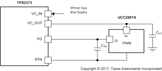
The PG pin can be used to inhibit downstream converter startup by keeping the soft-start pin low. Figure 21 shows an example where PG connects to the SS pin of a DC-DC controller. Because PG is an open drain output, it will not affect the soft-start capacitor charge time when it deasserts. Another common use of the PG pin is to enable a converter with an active-high enable input. In this case, PG may require a pullup resistor to either VDD, or to a bias supply, depending on the requirements of the controller enable pin.
 Figure 21. PG Interface