SLUSCD1C June 2017 – November 2018 TPS2373
PRODUCTION DATA.
- 1 Features
- 2 Applications
- 3 Description
- 4 Revision History
- 5 Pin Configuration and Functions
- 6 Specifications
-
7 Detailed Description
- 7.1 Overview
- 7.2 Functional Block Diagram
- 7.3
Feature Description
- 7.3.1 APD Auxiliary Power Detect
- 7.3.2 PG Power Good (Converter Enable) Pin Interface
- 7.3.3 CLSA and CLSB Classification
- 7.3.4 DEN Detection and Enable
- 7.3.5 Internal Pass MOSFET
- 7.3.6 TPH, TPL and BT PSE Type Indicators
- 7.3.7 VC_IN, VC_OUT, UVLO_SEL, and Advanced PWM Startup
- 7.3.8 AMPS_CTL, MPS_DUTY and Automatic MPS
- 7.3.9 VDD Supply Voltage
- 7.3.10 VSS
- 7.3.11 Exposed Thermal PAD
- 7.4
Device Functional Modes
- 7.4.1 PoE Overview
- 7.4.2 Threshold Voltages
- 7.4.3 PoE Startup Sequence
- 7.4.4 Detection
- 7.4.5 Hardware Classification
- 7.4.6 Inrush and Startup
- 7.4.7 Maintain Power Signature
- 7.4.8 Advanced Startup and Converter Operation
- 7.4.9 PD Hotswap Operation
- 7.4.10 Startup and Power Management, PG and TPH, TPL, BT
- 7.4.11 Adapter ORing
- 7.4.12 Using DEN to Disable PoE
- 7.4.13 ORing Challenges
-
8 Application and Implementation
- 8.1 Application Information
- 8.2
Typical Application
- 8.2.1 Design Requirements
- 8.2.2
Detailed Design Requirements
- 8.2.2.1 Input Bridges and Schottky Diodes
- 8.2.2.2 Protection, D1
- 8.2.2.3 Capacitor, C1
- 8.2.2.4 Detection Resistor, RDEN
- 8.2.2.5 Classification Resistors, RCLSA and RCLSB
- 8.2.2.6 APD Pin Divider Network RAPD1, RAPD2
- 8.2.2.7 Opto-isolators for TPH, TPL and BT
- 8.2.2.8 VC Input and Output, CVCIN and CVCOUT
- 8.2.2.9 UVLO Select, UVLO_SEL
- 8.2.2.10 Automatic MPS and MPS Duty Cycle, RMPS and RMPS_DUTY
- 8.2.2.11 Internal Voltage Reference, RREF
- 8.2.3 Application Curves
- 9 Power Supply Recommendations
- 10Layout
- 11Device and Documentation Support
- 12Mechanical, Packaging, and Orderable Information
7.4.9 PD Hotswap Operation
IEEE802.3bt includes new PSE output limiting requirements for Type 3 and 4 operation to cover higher power and 4-pair applications. Type 2, 3 and 4 PSEs must meet an output current vs time template with specified minimum and maximum sourcing boundaries. The peak output current per each 2-pair may be as high as 50 A for 10 μs or 1.75 A for 75 ms, and the total peak current becomes twice these values when power is delivered over 4 pairs. This makes robust protection of the PD device even more important than it was in IEEE 802.3-2012.
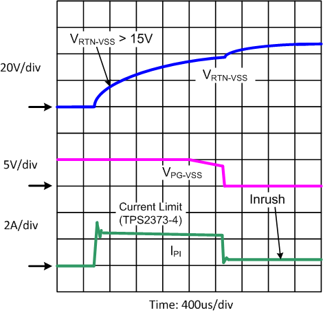
The internal hotswap MOSFET is protected against output faults and input voltage steps with a current limit and deglitched (time-delay filtered) foldback. An overload on the pass MOSFET engages the current limit, with V(RTN-VSS) rising as a result. If V(RTN-VSS) rises above approximately 14.5 V for longer than approximately 1.65 ms, the current limit reverts to the inrush value and PG output is forced low which turns off the converter, although there is no minimum inrush delay period (81.5-ms) applicable in this case. The 1.65-ms deglitch feature prevents momentary transients from causing a PD reset, provided that recovery lies within the bounds of the hotswap and PSE protection. Figure 28 shows an example of the RTN current profile during VDD to RTN short circuit, using 5-ohm load impedance. The hotswap MOSFET goes into current limit, causing the RTN voltage to increase. Once VRTN exceeds 14.5 V, IRTN, which was clamped to the current limit drops to the level of inrush current limit after 1.65 ms.
The inrush current limit is also reestablished when V(VDD-VSS) drops below UVLO then rises above it.
 Figure 28. Response to PD Output Short Circuit
 The PD control has thermal sensors that protect the internal hotswap MOSFET, the startup current source and the MPS pulsed current driver. Conditions like startup or operation into a VDD-to-RTN short cause high power dissipation in the MOSFET. An over-temperature shutdown (OTSD) turns off the hotswap MOSFET, the class regulator, the startup current source, and the MPS driver, which are restarted after the device cools. The hotswap MOSFET will be re-enabled and the TPS2373 will return to inrush phase when exiting from an overtemperature event. Pulling DEN to VSS during powered operation causes the internal hotswap MOSFET to turn off. This feature allows a PD with option three ORing per Figure 29 to achieve adapter priority.
The hotswap switch will be forced off under the following conditions:
- VAPD above VAPDEN (approximately 1.65 V),
- V(DEN –VSS) < VPD-DIS when V(VDD-VSS) is in the operational range,
- PD is over-temperature, or
- V(VDD –VSS) < PoE UVLO falling threshold (approximately 32 V).