SLUUBA2B March   2015  – November 2015 BQ25890 , BQ25892 , BQ25895 , BQ25895M , BQ25896


  1.   bq25890EVM, bq25892EVM, bq25895EVM, bq25896EVM and bq25895MEVM(PWR664)
    1.     Trademarks
    2. 1 Introduction
      1. 1.1 EVM Features
      2. 1.2 I/O Descriptions
    3. 2 Test Summary
      1. 2.1 Equipment
      2. 2.2 Equipment Setup
      3. 2.3 Procedure
        1. 2.3.1 Communication Verification
        2. 2.3.2 Charger Mode Verification
        3. 2.3.3 Boost Mode Verification
        4. 2.3.4 Helpful Hints
    4. 3 PCB Layout Guideline
    5. 4 Board Layout, Schematic, and Bill of Materials
      1. 4.1 PWR664 PCB Layouts
      2. 4.2 Schematics
      3. 4.3 Bill of Materials
  2.   Revision History

Communication Verification

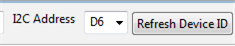
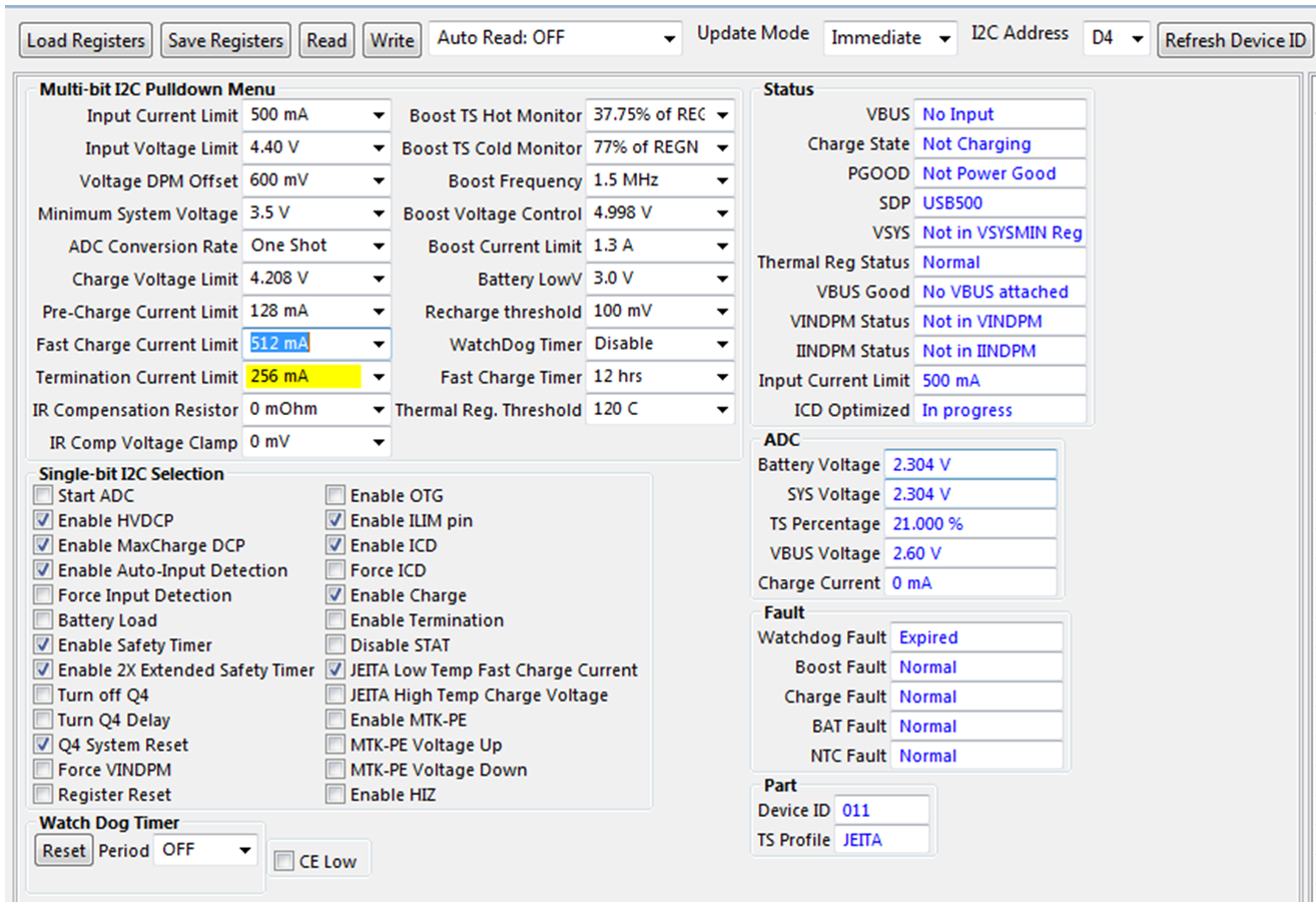
  1. In the EVM software, specify device “I2C Address” as D6 for bq25892/6, and D4 for bq25890/5.
  2. fig06_sluuba2.gif
  3. Enable Load#1 from Section 2.2, step 4. Click the Read button
  4. In the EVM GUI software (see example screen shot below) , make the following changes as necessary:
    • Select “Disabled” for the “Watchdog Timer”
    • Select "Force VINDPM"
    • Set “Input Voltage Limit” to 4.2
    • Set “Input Current Limit” to 500 mA
    • Set “Charge Voltage Limit” to 4.208 V
    • Set “Fast Charge Current” ICHG to 960 mA
    • Set "Minimum System Voltage" to 3.5V
    • Set “Pre-Charge Current” to 256 mA
    • Select "Charge Enable"
    • Deselect "Enable ILIM pin"
    • Deselect "Enable ICD"
    • Deselect “Enable Termination”
  5. nfig07a_main_eval_change_win_sluuba2.png