SLUUBA2B March   2015  – November 2015 BQ25890 , BQ25892 , BQ25895 , BQ25895M , BQ25896


  1.   bq25890EVM, bq25892EVM, bq25895EVM, bq25896EVM and bq25895MEVM(PWR664)
    1.     Trademarks
    2. 1 Introduction
      1. 1.1 EVM Features
      2. 1.2 I/O Descriptions
    3. 2 Test Summary
      1. 2.1 Equipment
      2. 2.2 Equipment Setup
      3. 2.3 Procedure
        1. 2.3.1 Communication Verification
        2. 2.3.2 Charger Mode Verification
        3. 2.3.3 Boost Mode Verification
        4. 2.3.4 Helpful Hints
    4. 3 PCB Layout Guideline
    5. 4 Board Layout, Schematic, and Bill of Materials
      1. 4.1 PWR664 PCB Layouts
      2. 4.2 Schematics
      3. 4.3 Bill of Materials
  2.   Revision History

Charger Mode Verification

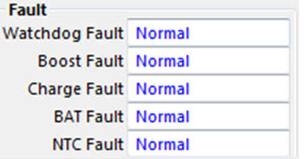
  1. Turn on PS#1, click the Read button twice:
    • Observe → Everything Normal at Fault box
    • nfig07b_sec7.2.1_sluuba2.png
    • Observe → D3 (STAT) is on
    • Observe → D4 (PG) is on (bq25892/6)
  2. Measure the voltage across J3 and J4 as follows:
    • Measure → V(TP4(SYS), TP7(GND)) = 3.65 V ±300 mV
    • Measure → V(TP5(BAT), TP7(GND)) = 2.5 V ±200 mV
  3. Change load to 3.7 V
    • Measure → I(BAT) = 625 mA ± 100 mA
    • Measure → V(TP5(BAT), TP7(GND)) = 3.7 V ±200 mV
    • Measure → I(VBUS) = 500 mA ± 200mA