SLUUCB5E June 2020 – July 2022 BQ25792 , BQ25798
2.4.4 OTG Mode Verification
Use the following steps for OTG mode verification for boost operation:
- Power up then turn off Load#2 output. Set to CR = 12 V/0.5 A = 24 Ω. Disconnect PS1 from J1 and attach Load#2 to J1 (VIN1 and GND).
- Increase Load #1 regulation
voltage to 8.0 V and take measurements as follows:
- Measure ➡ VBAT-PGND (TP27 and TP46) = 8.0 V ±0.1 V
- For BQStudio, prepare the OTG
mode charger register settings in the following way:
- On the 8-bit
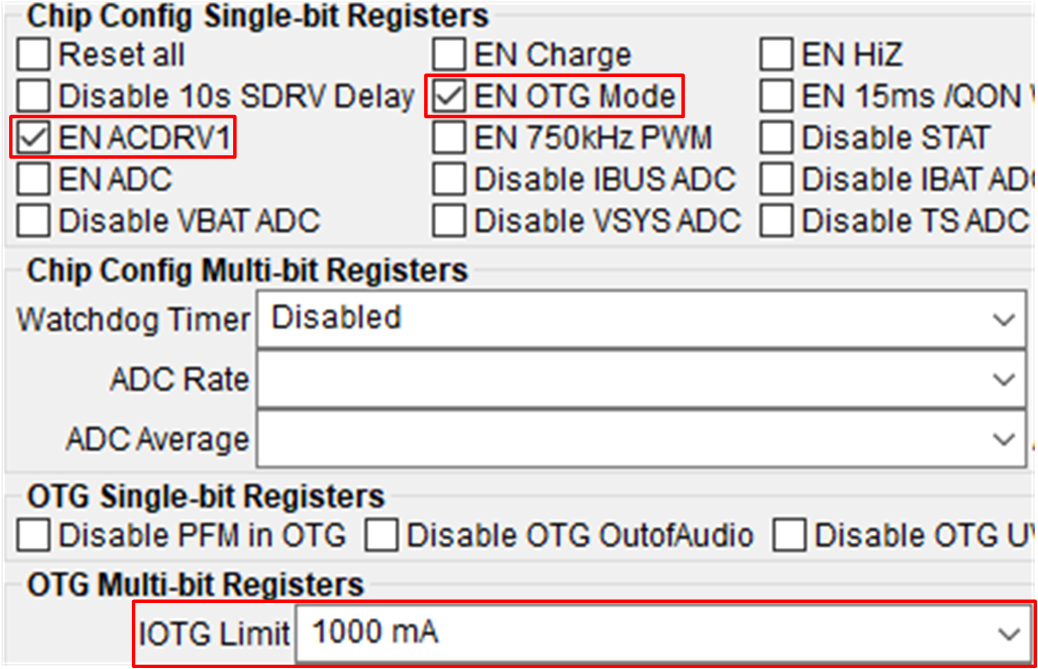
Registers tab in the Chip Config Single-bit Registers
section:
- Check the EN OTG Mode box
- Check the EN ACDRV1 box
- On the 8-bit
Registers tab in the OTG Multi-bit Registers section:
- Set IOTG 1000
mA to change the OTG current limit.
 Figure 2-8 Single-Bit Register Section
- Set IOTG 1000
mA to change the OTG current limit.
- On the 16-bit
Registers tab in the OTG Multi-bit Registers section:
- Set the OTG
mode regulation voltage to 12000 mV
 Figure 2-9 Multi-Bit Register Section
- Set the OTG
mode regulation voltage to 12000 mV
- OTG Reg Voltage to 12 V
- IOTG Limit to 1 A.
 Figure 2-10 OTG
Configuration Section
 Figure 2-11 Chip
Configuration
 - On the 8-bit
Registers tab in the Chip Config Single-bit Registers
section:
- Take measurements as follows:
- Measure ➡ VVBUS-PGND (TP21 and TP45) = 12.0 V ±0.2 V
- Measure ➡ VAC1-PGND (TP22 and TP45) = 12.0 V ±0.2 V
- Click READ ALL
REGISTERS
- Verify ➡ REG1Bb[6] reports VINDPM or OTG
- Verify ➡ REG1Cb[4:1] reports VBUS Status as Normal OTG
- Turn on Load#2 output set to CR of 24 Ω.
- Take measurements as follows:
- Measure ➡ VAC1-PGND (TP22 and TP45) = 12.0 V ±0.2 V
- Measure ➡ IAC1-SENSE (TP1 and TP2) = 500 mA ±0.10 A
- Lower the Load#2 CR to 10 Ω.
- Take measurements as follows to
confirm OTG current function:
- Measure ➡ VAC1-PGND (TP22 and TP45) < 12.0 V ±0.2 V
- Measure ➡ IAC1-SENSE (TP1 and TP2) = 1000 mA ±0.10 A
- Click READ ALL REGISTERS and Verify ➡ REG1Bb[7] reports IINDPM
- Hints for further OTG testing:
- Enabling OTG mode is a two-step process, first enable OTG and then turn on the appropriate AC drive FETs.