SLVA773 May 2016 LM2700 , TLV61220 , TPS61020 , TPS61024 , TPS61025 , TPS61026 , TPS61027 , TPS61028 , TPS61029 , TPS61030 , TPS61031 , TPS61032 , TPS61046 , TPS61070 , TPS61071 , TPS61072 , TPS61073 , TPS61088 , TPS61089 , TPS61090 , TPS61091 , TPS61092 , TPS61093 , TPS61098 , TPS61200 , TPS61201 , TPS61202 , TPS61220 , TPS61221 , TPS61222 , TPS61230 , TPS61232 , TPS61240 , TPS61241 , TPS61251 , TPS61252 , TPS61253 , TPS61254 , TPS61256 , TPS61258 , TPS61259 , TPS61260 , TPS61261
1 Introduction
Copying the layout of the boost converter from its datasheet or evaluation module (EVM) is easiest, but the layout may not fit the system board. So this application note details five steps that help to design a good PCB layout for the TPS61xxx converter. A high-current boost converter, TPS61236 as shown in Figure 1 is taken as the example to demonstrate the five steps.
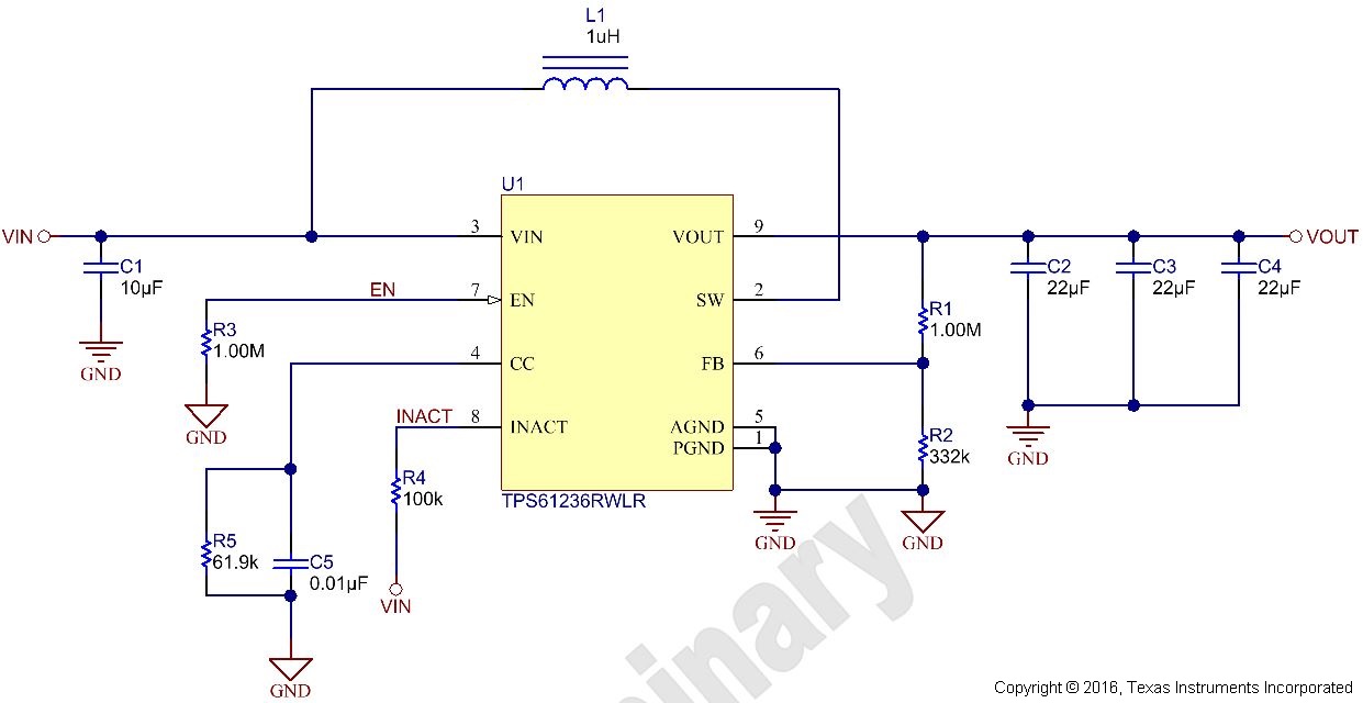 Figure 1. TPS61236 Schematic
 - Place and Route the Output Capacitor
- Place and Route the Inductor and Snubber
- Place and Route the Input Capacitor and VIN Pin
- Place and Route the Small Signal Components
- Connect the Signal Ground and Place Polygon Plane
The output capacitor location is the most important for any boost converter, so it should be placed close to the IC. Route the capacitor to the IC with short and wide trace to minimize the parasitic inductance. The reason is that the current flowing through the output capacitors is pulse-type[1]. Considering the V = L × dI / dt, the parasitic inductance between the IC and the output capacitors would cause voltage spike and ringing at the SW pin. Too high voltage spike can damage the IC and the ringing causes EMI problems.
Figure 2 shows how to place and route the output capacitors for the TPS61236. In the left, the three 0805 package capacitors are placed in parallel. This way is easy and has very small parasitic inductance. But sometimes, it is not easy to place the large package capacitors close to the IC because of the restriction of the system board. Then a small package capacitor can be placed near the IC and the bulk capacitors are placed somewhere farther. The bulk capacitor can be connected with the IC through relative long trace and vias, as shown in the right of Figure 2.
It is suggested to use one via per amp of current if the via is required[2]. More vias help to reduce parasitic resistance if room allows. In both cases, make sure the traces between the IC and output capacitor are wide enough to support the large current.
 Figure 2. Place and Route the Output Capacitors
 The second component to be placed is the inductor. To reduce the radiated EMI, the inductor should be placed close to the IC. The copper of the SW-node should be optimized to handle the large current with minimum area. The SW-node is the noisy source of the boost converter, so any trace of a sensitive node, such as FB, should be far away from the SW node. Figure 3 shows the placement and routing of the inductor in the two conditions.
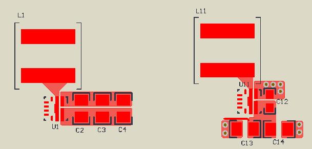 Figure 3. Place and Route the Inductor
 Snubber circuit in the SW-node is unnecessary for the normal operation of a boost converter. But it is occasionally required to reduce the EMI by damping the ringing and slowing down the voltage rising and falling edge at the SW-node. To be effective, the loop area of the snubber circuit (Rs and Cs) should be as small as possible to minimize the parasitic inductance, as shown in Figure 4.
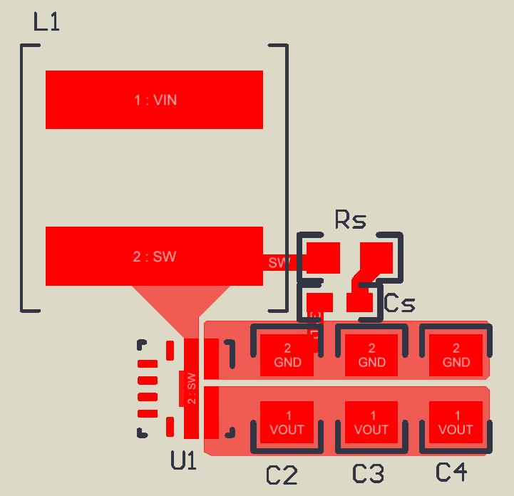 Figure 4. Place and Route of the Snubber Circuit
 The input capacitor is the final power component to be placed. The input capacitor is also used to power the internal control circuit and the input voltage detection circuit for undervoltage lockout (UVLO). So the ground-node of the input capacitor should be close to the IC power ground pin. The input capacitor ground-node, output capacitor ground-node and the IC ground-pin form a Power-Ground of the boost converter. The distance between VIN-node of the input capacitor and inductor is not important because the current through the input capacitor is continuous.
The VIN voltage is usually stable voltage, so a large VIN-node copper area would not cause trouble and a large copper area can help to improve the thermal performance. Figure 5 shows the placement of the input capacitor without and with a snubber circuit. The snubber circuit is more important than input capacitor, so it should be placed first, if required. As the snubber circuit is unnecessary for most of the application conditions, it will be not included in the following chapters.
The VIN pin of the IC can be connected with the VIN-node of the input capacitor through vias and direct trace in another layer because the current through this trace is small. If this trace is too long, a small decoupling capacitor can be placed closed to the VIN pin of the IC.
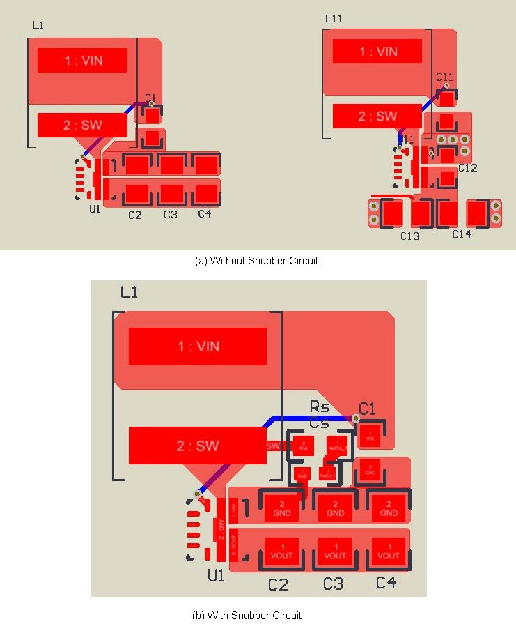 Figure 5. Place and Route the Input Capacitor and VIN Pin
 The small signal components include both the analog and logic components. For the TPS61236 boost converter, the small signal analog components are the resistors and capacitors (R1, R2, R5, C5) for the CC and FB pin. The small signal logic components are the resistors (R3, R4) for INACT and EN pin.
The analog components and nodes are sensitive to noise, especially when they have large input impedance, such as FB pin. Make sure these components are close to the IC. The traces between the components and IC should be short to minimize the parasitic capacitance with noisy SW node. Never route the FB trace in parallel with the SW node closely; otherwise the switching noise would couple to the FB pin and cause problems. Figure 6 shows the layout of the small signal analog components.
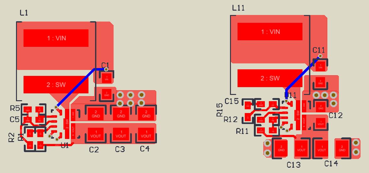 Figure 6. Place and Route of Analog Small Signal Components
 The logic circuit for EN and INACT pins is less important. The circuits normally have relatively small impedance and small voltage noise at these pins does not cause abnormal operation. These components are placed and routed last. As shown in Figure 7, the resistors are connected with the IC pins through vias and trace in another layer.
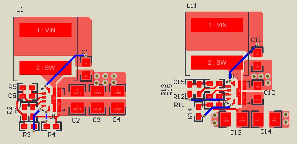 Figure 7. Place and Route the Logic Components
 The ground-node of the analog small signal components and AGND pin of the IC form a Signal-Ground, which must be connected to the Power-Ground of the IC through a single point. The single point should be closed to the PGND pin. Make sure no large power current is flowing through the Signal-Ground. Otherwise, noise coupling into the control circuit could causes bad output voltage regulation, inaccurate current limit, or other abnormal behaviors. Figure 8 shows a good example of Signal-Ground and Power-Ground connection.
 Figure 8. Route the Signal Ground
 The ground-nodes of the logic circuits are normally connected to the Signal-Ground as in Figure 8. But they can also be connected to Power-Ground if they are too far away from the Signal-Ground. Just make sure the voltage noise coupling into the logic circuit is not too high to interfere the logic behavior.
The IC mainly dissipates heat through the VOUT and GND pin. The large copper plane in these pins helps to improve thermal performance. TI recommends increasing the copper area as large as possible in the GND layer as shown in Figure 9. Thick copper, vias between the top layer and the bottom layer, and thin dielectric layer also help to improve the thermal performance.
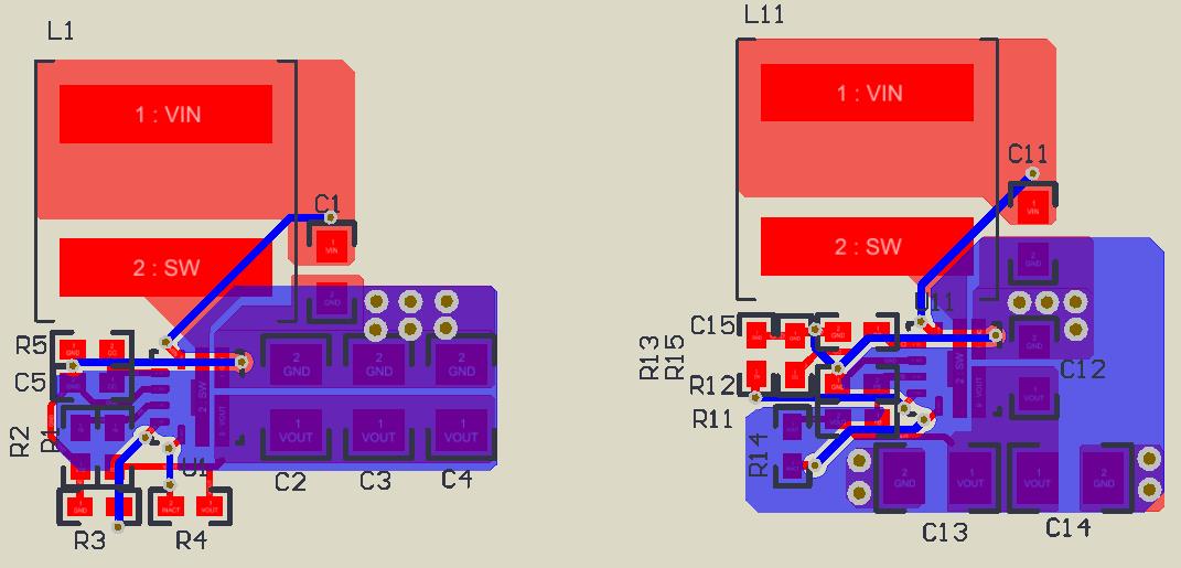 Figure 9. Place the Ground Polygon Plane
 The Signal-Ground can be connected to the ground plane directly without large power current flowing through the Signal-Ground, as shown in Figure 10 . In Figure 10, the power current flows on the top layer in the left layout; and the power current flows at the right side of the plane in the right layout. Compared to Figure 9, Figure 10 has larger copper area to help the thermal performance.
 Figure 10. Place the Full Ground Plane