SLVAEG1A August 2019 – May 2021 TLV62568 , TLV62568A , TPS62840
3 Buck Converter Architectures
Architecture A: Buck Converter + LDO
 Figure 3-1 Architecture A Block Diagram
The first architecture to be discussed is a common solution, where a buck converter is followed by an LDO to reduce output voltage ripple in order to meet required output voltage accuracy.
The benefit of using this topology is that this solution keeps noise on sensitive rails low compared to a buck converter alone, due to the power supply rejection ratio (PSRR) of the LDO. When several LDOs are cascaded off a single buck converter to create multiple power rails, there is an added benefit.The magnitude of rejection, and the frequency of the output voltage ripple,are almost the same since there is only one switching converter sourcing the rails, rather than multiple switching converters sourcing the rails. With multiple switching converters, there is no correlation between output voltage frequency and magnitude, while the PSRR of an LDO is constant at a particular switching frequency and adds no switching elements.
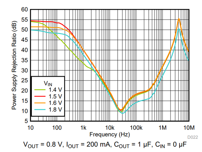
One thing worth noting when designing with this topology is the noise-filtering capability of the LDO. An LDO with high PSRR can be chosen for noise-sensitive rails. However, this PSRR changes with respect to the switching frequency and output current. Figure 3-2 shows an example of this for the TPS7A05, the LDO used in Architecture A. In general, an LDO has better noise attenuation at lower switching frequencies, (such as when the converter is in PFM operation) and worse noise attenuation at higher switching frequencies (such as when the converter is operating at nominal switching frequency). This being said, the PSRR at high frequencies can be improved by increasing the output capacitor value.
 Figure 3-2 PSRR Curve of TPS7A05 at 200 mA Load Current and 0.8 V Output Voltage
One other thing to be aware of is the efficiency of the LDO, which can be calculated as shown in Equation 2. With higher voltage drop comes lower system efficiency, causing the power tree to draw more current from the battery at all load levels and ultimately decrease the battery life. As shown in Equation 3 and Equation 4, higher voltage drop also causes a higher temperature within the LDO IC itself, which is something to be especially aware of in designs that need to meet outdoor operating temperature requirements.
One other LDO to consider for use with this architecture is the TPS7A02, which has an ultra-low nominal IQ of 25 nA, even in dropout. TPS7A02 is also optimized for excellent transient performance, and features a smart enable circuit with an internally controlled pulldown resistor to help minimize the external components used to pulldown the enable pin.
Architecture B: FPWM Buck Converter
 Figure 3-3 Architecture B Block Diagram
The second architecture is a simple solution for applications concerned with noise. An efficient switching converter is forced to stay in PWM mode at light loads, rather than enter the power-saving PFM mode. In PFM mode, the converter only operates in short bursts when the output voltage falls below the nominal output voltage. This saves power by only turning on and switching when the minimum output voltage threshold is crossed, which reduces switching losses.
For buck converters that operate in both PFM and PWM modes, varying ripple voltage and frequency can be seen in dynamic load conditions as the buck converter changes operating mode from PFM to PWM, or vice versa. This behavior is not seen in the FPWM device, as it is forced to stay in PWM mode regardless of the load applied. As such, the benefit of a FPWM buck converter is that the switching frequency does not change, giving a fairly constant ripple for a fixed output capacitor, and improving the transient response across load variations. Additionally, the system efficiency at full load is much higher than the previous cascaded architecture, since no LDO is present.
The disadvantage of this architecture is a high IQ and low light-load efficiency. Both of these disadvantages are direct results of the FPWM mode. Because the device remains in PWM mode regardless of the load conditions, the device continues to switch at high frequency and draw higher current even at no load, which causes a high IQ. For the same reason, the light-load efficiency is extremely low since the current drawn by the buck converter is much higher than the output current at light loads.
Architecture C: Buck Converter + PI Filter
 Figure 3-4 Architecture C Block Diagram
The third and final architecture to be discussed is a high-performance solution where a noise-sensitive rail is powered by an efficient switching converter to generate the desired voltage. As shown in Figure 3-4, it is followed by a ferrite bead PI filter to attenuate the switching noise. In this configuration, the buck converter can operate in the power-saving PFM mode, which allows for higher efficiency in light load conditions as previously discussed.
Implementing this architecture results in the lowest and most consistent output voltage ripple for full load conditions, which makes it the most ideal for peripherals with tight power supply noise requirements. Because these peripherals have the most stringent power supply regulation requirements when they are powered and actively processing data, full load noise levels are more important than light load noise levels, as light loads typically correspond to a peripheral in standby or shutdown mode.
In addition to low noise, this architecture provides high efficiency at all load levels. Similar to Architecture B, this topology is comprised of a single buck converter and no LDO, so the system efficiency is much higher than a power architecture using one or more LDOs. Unlike Architecture B, the noise requirement is handled externally by the buck converter with a PI filter, which allows the converter to operate in PFM mode and increases efficiency in light load conditions.
There are some considerations to take in the process of designing with this architecture. It is necessary to calculate the frequency and magnitude of the output voltage ripple of the buck converter for operating load conditions of the peripherals in order to design the PI filter, and there are further calculations in choosing the ferrite bead and passives around it. Implementing the PI filter is not quite as simple as implementing an LDO, which requires choosing an adequate PSRR at the nominal switching frequency of the buck converter. Additionally, the PI filter has a more limited bandwidth for rejection, and has slight variations in settling time, which is a function of the filter values.
For this design, a ferrite bead is used and the following values chosen for the PI filter:
- CIN = 0.1 µF
- COUT = 10 µF
- RDAMP = 0.33 Ω
- CDAMP = 47 µF
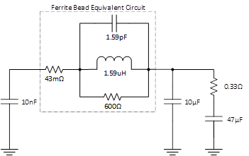
The PI filter design is done using equations and criteria from TIDA-01579.Figure 3-5 shows the filter circuit and the equivalent circuit of the ferrite bead.
 Figure 3-5 PI Filter Circuit Diagram