SLVAER0B August 2020 – December 2020 TPS55288 , TPS55288-Q1 , TPS552882 , TPS552882-Q1
2.1 Identification of the Critical Switching Loops
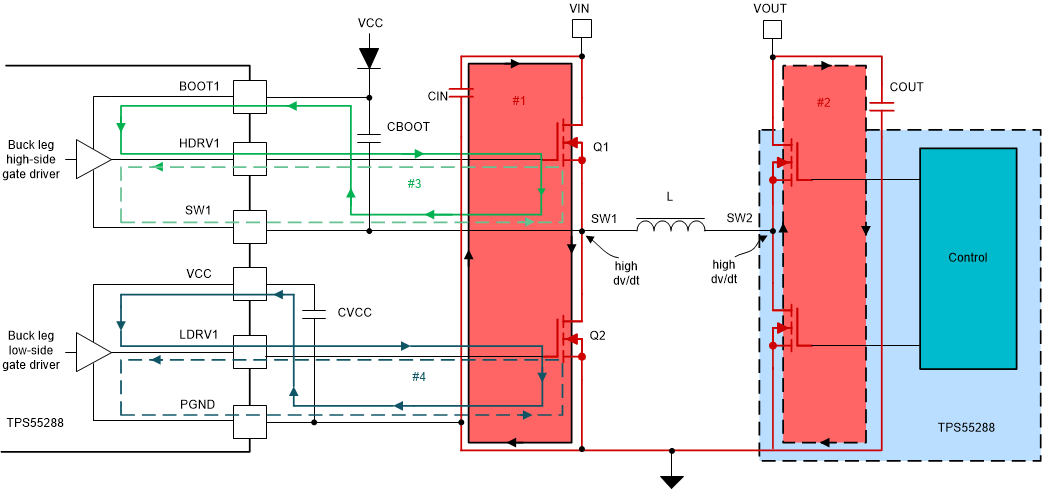
Figure 2-1 shows the TPS55288 four-switch buck-boost converter with power stage components, an integrated gate drivers and a VCC bias supply. Figure 2-1 also distinguishes by color the high current traces, high dI/dt critical loops, and the high dv/dt switching nodes.
 Figure 2-1 Buck-Boost Converter Schematic With Critical Loops
Loop 1 and loop 2, shaded in red, are the two critical high-frequency power loops for the buck-legs and the boost-legs. Long and thin traces in these two loops can cause excessive noise, overshoot, and ring on the switch node, and the ground bounce because of the parasitic inductance. During a MOSFET switching event, the slew rate of the commutating current can exceed 3–5 A/ns, so a 2-nH parasitic inductance can result in a voltage spike of 6 V. The pulsed rectangular current waveforms flowing in these critical loops are rich in harmonic content, so a big loop area can cause big radiated energy emanating from it, which causes an electromagnetic interference issue. So it is vital to minimize the trace length and the enclosed area of loop 1 and loop 2.
The current flowing in the main inductor is largely DC, with a superimposed triangular current ripple. The inductance inherently limits the current change rate. The parasitic inductance in series with the main inductor is benign. At the meanwhile, the area of the switching node SW1 and SW2 should be as small as possible. If the SW1 and SW2 are poured with big area copper planes, the high dv/dt noisy signal will couple into other traces nearby though capacitive coupling, which causes the electromagnetic interference issue.
Loop 3 and loop 4 in Figure 2-1 are gate loops for the buck-leg MOSFET. Loop 3 represents the high-side gate driver circuits of the MOSFET supplied by the bootstrap capacitor. Loop 4 represents the low side gate driver circuits of the MOSFET supplied by the VCC capacitor. The turn-on path and the turn- off path are denoted by the solid and the dashed lines, respectively. To charge and discharge the gate capacitance of the MOSFET during turn-on and turn-off transitions, an instantaneous current up to around 1-A peak flows briefly in the gate loop.
Placing the VCC decoupling capacitor very close to the VCC and PGND pins, placing the bootstrap capacitor very close to the SW and the boot pins can reduce the gate loop enclosed areas. Route the gate drive traces from the silicon to the MOSFET as short as possible, routing the gate drive and the return traces side by side can minimize the gate-loop inductance and the gate-loop area.