SLVAER0B August 2020 – December 2020 TPS55288 , TPS55288-Q1 , TPS552882 , TPS552882-Q1
2.2 Power Component Placement
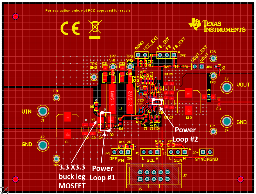
Figure 2-2 illustrates the placement of the power MOSFETs, input and output ceramic capacitors, main inductor, and the TPS55288 silicon on the top layer.
 Figure 2-2 Power Stage Components Placement
Input capacitors are placed close to the buck-leg MOSFETs. Output capacitors are placed adjacent to the TPS55288’s VOUT pin and PGND pin. A small enclosed area of the power loop 1 and power loop 2 can be achieved by proper placement.
The main inductor L1 is placed between the buck-leg MOSFETs and the TPS55288 silicon. The SW node is poured with small copper plane to reduce the capacitive coupling relating to the SW node high dv/dt transitions. A large SW node copper plane helps the thermal, but will cause severe radiated emissions.