SLVAEX2 September 2020 – MONTH TPS55288 , TPS55288-Q1 , TPS552882 , TPS552882-Q1
2.3.5 Adding Filters at the Input and Output Side
The discontinuous currents are present at the input and the output side of the buck-boost converter. Voltage ripple generated by the discontinuous current can be conducted to other systems via input and output cables or PCB traces. The selection of the input filter inductor and the output beads are based on the initial EMI noise test result.
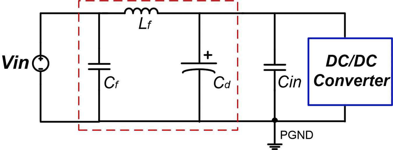
When the converter works under the buck mode, generally CLC EMI filter should be added at the input side, see Figure 2-12. Many papers and articles write about this input filter design [3]. The typical procedure includes identify the noise level at the switching frequency, calculate the required attenuation, select the Lf and Cf, then calculate the damping capacitance Cd.
 Figure 2-12 Simplified Input EMI
Filter
Figure 2-12 Simplified Input EMI
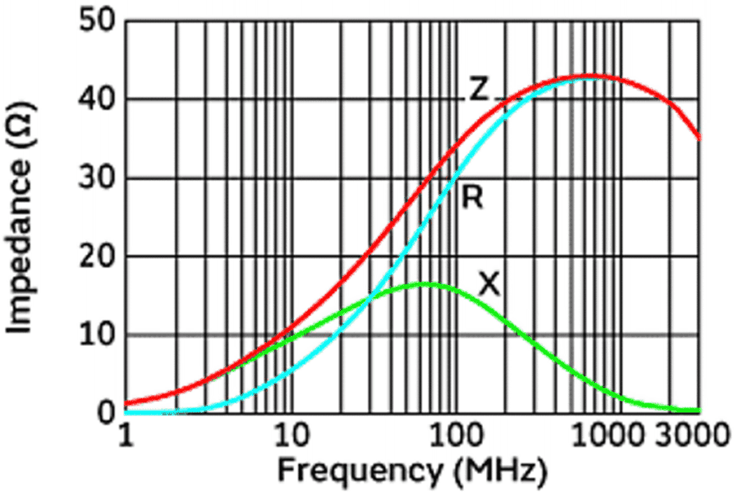
FilterWhen the converter works under the boost mode, ferrite beads are generally added at the output side. When selecting a bead, we should carefully study the impedance versus frequency characteristics when choosing a ferrite bead. Make sure the bead’s resistive impedance is much higher than the reactive impedance in the noise frequency range. Figure 2-13 shows the Murata part BLM21PG300SN1’s impedance versus frequency characteristic. We can see that this bead can provide optimum performance at noise frequencies from 100 MHz to 3 GHz range.
 Figure 2-13 Impedance Characteristics of
BLM21PG300SN1