SLVAFQ1 October 2023 TPS541620 , TPS543320 , TPS543620 , TPS543820 , TPS546D24A , TPS548A28 , TPS548A29 , TPS563252 , TPS563257 , TPS568231 , TPS62912 , TPS62913 , TPSM5D1806 , TPSM82912 , TPSM82913 , TPSM843320 , TPSM863252 , TPSM863257 , TPSM8A28 , TPSM8A29
A higher real-time sample rate and portability are two major trends for new oscilloscope products, along with more powerful digital circuits and a smaller board size. To support this, power systems with better dynamic load performance and higher power density are preferred. Low noise and low output ripple are also required by sensitive analog components for generating high-accuracy images. Although 12 V is still the most common intermediate rail, 24-V architectures are becoming increasingly popular. In this article, common design challenges associated with using buck regulators for oscilloscope power are discussed.
| GPN | VIN | IOUT | Fsync | Features | Module Option | |
|---|---|---|---|---|---|---|
| Fast Transient Response | TPS563252 | 3 V–17 V | 3 A | Fast transient response, Ease of use, 1.2 MHz 3 A, wide range of VOUT, ECO/FCCM/OOA | TPSM863252 | |
| TPS563257 | 3 V–17 V | 3 A | TPSM863257 | |||
| TPS568231 | 3.8 V–17 V | 8 A | Fast transient response, P2P 8 A/12 A family, 400/800/1200 KHz, ECO/FCCM, Adj soft start | |||
| TPS56C231 | 3.8 V–17 V | 12 A | ||||
| TPS548A28 | 2.7 V–16 V | 15 A | Fast transient response, P2P 15/20-A family, 600/800/1000 KHz, Adj soft start | TPSM8A28 | ||
| TPS548A29 | 2.7 V–16 V | 20 A | TPSM8A29 | |||
|
High Power Density |
TPS543320 | 4 V–18 V | 3 A | √ | Highest efficiency 12 V/6 A converter in the market, P2P 3/6/8 A family, ±0.5 % accuracy, selectable Fsw: 500 KHz/750 KHz/1 MHz/1.5 MHz/2.2 MHz, Fsync. Power good, Adj soft start | TPSM843320 |
| TPS543620 | 4 V–18 V | 6 A | √ | TPSM843620 | ||
| TPS543820 | 4 V–18 V | 8 A | √ | TPSM843820 | ||
| TPS541620 | 4.5 V–15 V | Dual 6 A | √ | Dual-channel, Small size, 500 KHz/1 MHz/1.5 MHz/2 MHz, Adj soft start, Fsync | TPSM5D1806 | |
| TPS543A22 | 4 V–18 V | 12 A | √ | Highest power density 25-A converter, P2P12/16/20/25-A family, ±0.5 % accuracy, Selectable Fsw: 500 KHz/750 KHz/1 MHz/1.5 MHz/2.2 MHz, Fsync. Power good, Adj soft start | TPSM843A22 | |
| TPS543A26 | 4 V–18 V | 16 A | √ | TPSM843A26 | ||
| TPS543B22 | 4 V–18 V | 20 A | √ | TPSM843B22 | ||
| TPS543B25 | 4 V–18 V | 25 A | √ | |||
| Low noise | TPS62912 | 3 V–17 V | 2 A | √ |
Eliminates LDO and passive post filtering, low noise/ripple, Spread spectrum modulation,1 MHz/2.2 MHz, Fsync |
TPSM82912 |
| TPS62913 | 3 V–17 V | 3 A | √ | TPSM82913 | ||
|
Digital Interface |
TPS546D24A | 2.95 V–16 V | 40 A | √ | PMBus with telemetry, Stack x4, Over 90% efficiency 12 VIN, 1 VOUT, 500 kHz from 15 A–25 A. 275 KHz-1.5 MHz, Fsync | TPSM8D6C24 |
| TPS546B24A | 2.95 V–16 V | 20 A | √ | TPSM8D6B24 | ||
| TPS546A24A | 2.95 V–16 V | 10 A | √ | |||
| 24 V rails | TPS62933 | 3.8 V–30 V | 3 A | Wide VIN range, 200 KHz to 2.2 MHz selectable frequency, EN, Light load efficiency, Adj soft start, Spread spectrum modulation | ||
| TPS62932 | 3.8 V–30 V | 2 A | ||||
| TPS56637 | 4.5 V–28 V | 6 A | High efficiency, ECO/FCCM/OOA, Selectable Fsw: 500 KHz/800 KHz/1.2MHz, Large duty support, power good, Adj soft start | TPSM86638 | ||
| TPS56837 | 4.5 V–28 V | 8 A | TPSM86838 |
Challenges
Fast Transient Response for CPU and FPGA Core Voltage
When an oscilloscope is conducting signal sampling and processing, the load current drawn by digital circuits such as CPU and FPGA can change rapidly. To regulate the output voltage within a small range of undershoot and overshoot, power devices with fast transient response behavior are required in most oscilloscope power designs. Without this behavior, the CPU/FPGA can not receive a stable input voltage, decreasing system performance. A key device designed for solving this challenge is TPSM863257. Rather than requiring large output capacitance like a current mode regulator, TPSM863257 uses comparator-based D-CAP3TM control mode to achieve fast transient response, as shown in Figure 1, ΔVOUT within ±3 % VOUT. In addition, TPSM863257 is easy to use with minimized external components and is available for large-duty operation support.
 Figure 1 TPSM863257 Transient Response
with
12 V to 1.05 V, 0.3 A to 2.7 A, 1
A/μs
SR
Figure 1 TPSM863257 Transient Response
with
12 V to 1.05 V, 0.3 A to 2.7 A, 1
A/μs
SRNoise Emissions
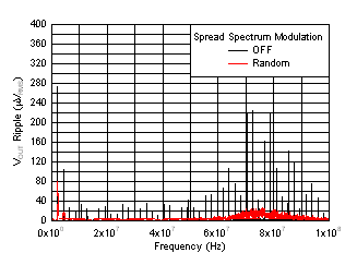
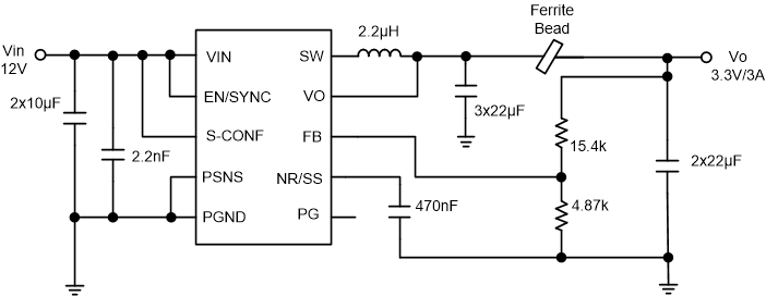
Because the ADCs, DACs and AFEs in oscilloscopes are sensitive to the radiated emissions, low noise buck regulators with less EMI emission are preferred. TPS62913 and TPSM82913 are designed for low EMI options for 12-V input rails. TPS62913 and TPSM82913 can support frequency spread spectrum modulation, which helps with lowering EMI noise. Spread spectrum eliminates peak emissions at specific frequencies by spreading emissions across a wider range of frequencies than a part with fixed frequency operation. Compared with a traditional switching regulator + LDO option, TPS62913 and TPSM82913 can achieve less than 20-μVrms noise in a single chip option. And less than 10-μVrms output ripple can also be achieved by implementing internal compensation of a ferrite beam filter, as shown in Figure 2 and Figure 3.
 Figure 2 VOUT
Ripple FFT of TPS62913 at 12
VIN
to 3.3
VOUT,
2.2 MHz
 Figure 3 Typical Application with Integrated
Ferrite Bead Filter Compensation
Figure 3 Typical Application with Integrated
Ferrite Bead Filter CompensationPower Density
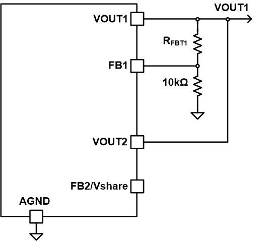
For both high-end and portable oscilloscopes' power designs, board area and height are becoming limiting factors as power demands increase. Power engineers must reduce their circuit design area and improve efficiency to achieve higher power density. TPSM5D1806 has input voltage ranging from 4.5 V to 15 V, an output current of dual 6 A and a small package size (5.5 mm × 8 mm × 1.8 mm), which can help to achieve high power density and optimized design layout. When connecting the two outputs of TPSM5D1806 for current sharing, the module can supply up to 12 A, as shown in Figure 4. TPSM5D1806 also offers high efficiency and can achieve up to 92% at the condition of 12 VIN to 5 VOUT, 3-A output current and switching frequency of 2 MHz.
 Figure 4 Single Device, Current Sharing
Another challenge of oscilloscope power design is to monitor key parameters including output voltage and input current. Oscilloscopes need stable output voltage to verify the accuracy of signal measurement. By using buck regulators with PMBusTM interface with telemetry, you can monitor the real-time output voltage and adjust the voltage for stability. In addition, monitoring input current can help evaluate efficiency and optimize power management so as to extend battery life and reduce power consumption. Key PMBus-enabled device families designed for this challenge are the TPS546A24A family of converters and the TPSM8D6C24 family of modules.
TPS546A24A and TPSM8D6C24 are fixed frequency devices with selectable switching frequencies and are able to synchronize to the external clock, which can also help to achieve stable frequency. For TPSM8D6C24, there are a dual 35 A or single 70 A and up to a 4-phase stackable module. See the simplified application in Figure 5.
The Texas Instruments Fusion Digital Power Designer supports the TPS546A24A and TPSM8D6C24 devices. The Fusion Digital Power Designer is a graphical user interface (GUI), which can be used to configure and monitor the devices through the PMBus using a Texas Instruments USB-to-GPIO adapter. Download the Texas Instruments Fusion Digital Power Designer software package.
 Figure 5 Simplified Application of
TPSM8D6C24
Figure 5 Simplified Application of
TPSM8D6C24Conclusion
Designing power supplies for oscilloscopes requires consideration of transient response, noise emission, power density and power parameter monitoring. TI's broad portfolio of buck converters and modules is well-equipped to address all of these power design challenges in both 12-V and 24-V input rails with various output currents.