SLVS484C June 2003 – December 2014 TPS61090 , TPS61091 , TPS61092
PRODUCTION DATA.
- 1 Features
- 2 Applications
- 3 Description
- 4 Revision History
- 5 Device Comparison Table
- 6 Pin Configuration and Functions
- 7 Specifications
- 8 Parameter Measurement Information
- 9 Detailed Description
-
10Application and Implementation
- 10.1 Application Information
- 10.2
Typical Applications
- 10.2.1 Typical Application Circuit for Adjustable Output Voltage Option
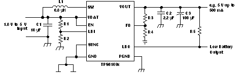
- 10.2.2 TPS6109x Application Schematic of 5 Vout With Maximum Output Power
- 10.2.3 TPS6109x Application Schematic of 5 Vout and Auxiliary 10 Vout With Charge Pump
- 10.2.4 TPS6109x Application Schematic of 5 Vout and Auxiliary -5 Vout With Charge Pump
- 11Power Supply Recommendations
- 12Layout
- 13Device and Documentation Support
- 14Mechanical, Packaging, and Orderable Information
1 Features
- Synchronous (96% Efficient) Boost Converter With 500-mA Output Current From 1.8-V Input
- Available in a 16-Pin VQFN 4 x 4 Package
- Device Quiescent Current: 20 µA (Typ)
- Input Voltage Range: 1.8 V to 5.5 V
- Adjustable Output Voltage Up to 5.5 V Fixed Output Voltage Options
- Power Save Mode for Improved Efficiency at Low Output Power
- Low Battery Comparator
- Low EMI-Converter (Integrated Antiringing Switch)
- Load Disconnect During Shutdown
- Over-Temperature Protection
2 Applications
- All Single Cell Li or Dual Cell Battery or USB Powered Operated Products
- MP3 Player
- PDAs
- Other Portable Equipment
3 Description
The TPS6109x devices provide a power supply solution for products powered by either a one-cell Li-Ion or Li-Polymer, or a two-cell alkaline, NiCd or NiMH battery and required supply currents up to or higher than 1 A. The converter generates a stable output voltage that is either adjusted by an external resistor divider or fixed internally on the chip. It provides high efficient power conversion and is capable of delivering output currents up to 0.5 A at 5 V at a supply voltage down to 1.8 V. The implemented boost converter is based on a fixed frequency, pulse-width- modulation (PWM) controller using a synchronous rectifier to obtain maximum efficiency. Boost switch and rectifier switch are connected internally to provide the lowest leakage inductance and best EMI behavior possible. The maximum peak current in the boost switch is limited to a value of 2500 mA.
The converter can be disabled to minimize battery drain. During shutdown, the load is completely disconnected from the battery. A low-EMI mode is implemented to reduce ringing and, in effect, lower radiated electromagnetic energy when the converter enters the discontinuous conduction mode.
The output voltage can be programmed by an external resistor divider or is fixed internally on the chip.
The device is packaged in a 16-pin VQFN 4-mm x 4-mm (16 RSA) package.
Device Information(1)
| PART NUMBER | PACKAGE | BODY SIZE (NOM) |
|---|---|---|
| TPS61090 | VQFN (10) | 4.00 mm × 4.00 mm |
| TPS61091 | ||
| TPS61092 |
- For all available packages, see the orderable addendum at the end of the datasheet.
Simplified Application Schematic