SLVS484C June 2003 – December 2014 TPS61090 , TPS61091 , TPS61092
PRODUCTION DATA.
- 1 Features
- 2 Applications
- 3 Description
- 4 Revision History
- 5 Device Comparison Table
- 6 Pin Configuration and Functions
- 7 Specifications
- 8 Parameter Measurement Information
- 9 Detailed Description
-
10Application and Implementation
- 10.1 Application Information
- 10.2
Typical Applications
- 10.2.1 Typical Application Circuit for Adjustable Output Voltage Option
- 10.2.2 TPS6109x Application Schematic of 5 Vout With Maximum Output Power
- 10.2.3 TPS6109x Application Schematic of 5 Vout and Auxiliary 10 Vout With Charge Pump
- 10.2.4 TPS6109x Application Schematic of 5 Vout and Auxiliary -5 Vout With Charge Pump
- 11Power Supply Recommendations
- 12Layout
- 13Device and Documentation Support
- 14Mechanical, Packaging, and Orderable Information
9 Detailed Description
9.1 Overview
The TPS6109x synchronous step-up converter typically operates at a 600-kHz frequency pulse width modulation (PWM) at moderate to heavy load currents. The converter enters power save mode at low load currents to maintain a high efficiency over a wide load. The power save mode can also be disabled, forcing the converter to operate at a fixed switching frequency. The TPS6109x family is based on a fixed frequency with multiple feed forward controller topology. Input voltage, output voltage, and voltage drop on the NMOS switch are monitored and forwarded to the regulator. The peak current of the NMOS switch is also sensed to limit the maximum current flowing through the switch and the inductor. It can also operate synchronized to an external clock signal that is applied to the SYNC pin. Additionally, TPS6109x integrated the low-battery detector circuit typically used to supervise the battery voltage and to generate an error flag when the battery voltage drops below a user-set threshold voltage.
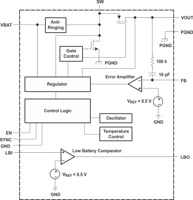
9.2 Functional Block Diagram
9.3 Feature Description
9.3.1 Synchronous Rectifier
The device integrates an N-channel and a P-channel MOSFET transistor to realize a synchronous rectifier. Because the commonly used discrete Schottky rectifier is replaced with a low RDS(ON) PMOS switch, the power conversion efficiency reaches 96%. To avoid ground shift due to the high currents in the NMOS switch, two separate ground pins are used. The reference for all control functions is the GND pin. The source of the NMOS switch is connected to PGND. Both grounds must be connected on the PCB at only one point close to the GND pin. A special circuit is applied to disconnect the load from the input during shutdown of the converter. In conventional synchronous rectifier circuits, the backgate diode of the high-side PMOS is forward biased in shutdown and allows current flowing from the battery to the output. This device however uses a special circuit which takes the cathode of the backgate diode of the high-side PMOS and disconnects it from the source when the regulator is not enabled (EN = low).
The benefit of this feature for the system design engineer is that the battery is not depleted during shutdown of the converter. No additional components have to be added to the design to make sure that the battery is disconnected from the output of the converter.
9.3.2 Controller Circuit
The controller circuit of the device is based on a fixed frequency multiple feedforward controller topology. Input voltage, output voltage, and voltage drop on the NMOS switch are monitored and forwarded to the regulator. So changes in the operating conditions of the converter directly affect the duty cycle and must not take the indirect and slow way through the control loop and the error amplifier. The control loop, determined by the error amplifier, only has to handle small signal errors. The input for it is the feedback voltage on the FB pin or, at fixed output voltage versions, the voltage on the internal resistor divider. It is compared with the internal reference voltage to generate an accurate and stable output voltage.
The peak current of the NMOS switch is also sensed to limit the maximum current flowing through the switch and the inductor. The typical peak current limit is set to 2200 mA.
An internal temperature sensor prevents the device from getting overheated in case of excessive power dissipation.
9.3.3 Device Enable
The device is put into operation when EN is set high. It is put into a shutdown mode when EN is set to GND. In shutdown mode, the regulator stops switching, all internal control circuitry including the low-battery comparator is switched off, and the load is isolated from the input (as described in the Synchronous Rectifier Section). This also means that the output voltage can drop below the input voltage during shutdown. During start-up of the converter, the duty cycle and the peak current are limited in order to avoid high peak currents drawn from the battery.
9.3.4 Undervoltage Lockout
An undervoltage lockout function prevents device start-up if the supply voltage on VBAT is lower than typically 1.6 V. When in operation and the battery is being discharged, the device automatically enters the shutdown mode if the voltage on VBAT drops below approximately 1.6 V. This undervoltage lockout function is implemented in order to prevent the malfunctioning of the converter.
9.3.5 Softstart
When the device enables the internal startup cycle starts with the first step, the precharge phase. During precharge, the rectifying switch is turned on until the output capacitor is charged to a value close to the input voltage. The rectifying switch current is limited in that phase. This also limits the output current under short-circuit conditions at the output. After charging the output capacitor to the input voltage the device starts switching. Until the output voltage is reached, the boost switch current limit is set to 40% of its nominal value to avoid high peak currents at the battery during startup. When the output voltage is reached, the regulator takes control and the switch current limit is set back to 100%.
9.3.6 Power Save Mode and Synchronization
The SYNC pin can be used to select different operation modes. To enable power save, SYNC must be set low. Power save mode is used to improve efficiency at light load. In power save mode the converter only operates when the output voltage trips below a set threshold voltage. It ramps up the output voltage with one or several pulses and goes again into power save mode once the output voltage exceeds the set threshold voltage. This power save mode can be disabled by setting the SYNC to VBAT.
Applying an external clock with a duty cycle between 30% and 70% at the SYNC pin forces the converter to operate at the applied clock frequency. The external frequency has to be in the range of about ±20% of the nominal internal frequency. Detailed values are shown in the electrical characteristic section of the data sheet.
9.3.7 Low Battery Detector Circuit—LBI/LBO
The low-battery detector circuit is typically used to supervise the battery voltage and to generate an error flag when the battery voltage drops below a user-set threshold voltage. The function is active only when the device is enabled. When the device is disabled, the LBO pin is high-impedance. The switching threshold is 500 mV at LBI. During normal operation, LBO stays at high impedance when the voltage, applied at LBI, is above the threshold. It is active low when the voltage at LBI goes below 500 mV.
The battery voltage, at which the detection circuit switches, can be programmed with a resistive divider connected to the LBI pin. The resistive divider scales down the battery voltage to a voltage level of 500 mV, which is then compared to the LBI threshold voltage. The LBI pin has a built-in hysteresis of 10 mV. See the application section for more details about the programming of the LBI threshold. If the low-battery detection circuit is not used, the LBI pin should be connected to GND (or to VBAT) and the LBO pin can be left unconnected. Do not let the LBI pin float.
9.3.8 Low-EMI Switch
The device integrates a circuit that removes the ringing that typically appears on the SW node when the converter enters discontinuous current mode. In this case, the current through the inductor ramps to zero and the rectifying PMOS switch is turned off to prevent a reverse current flowing from the output capacitors back to the battery. Due to the remaining energy that is stored in parasitic components of the semiconductor and the inductor, a ringing on the SW pin is induced. The integrated antiringing switch clamps this voltage to VBAT and therefore dampens ringing.
9.4 Device Functional Modes
Table 2. TPS61090 Operation Mode
| MODE | DESCRIPTION | CONDITION |
|---|---|---|
| PWM | Boost in normal switching operation | SYNC pin is high, across whole load SYNC pin is low, medium to heavy load. |
| PFM | Boost in power save operation | SYNC pin is low, light load. |