SLVS484C June 2003 – December 2014 TPS61090 , TPS61091 , TPS61092
PRODUCTION DATA.
- 1 Features
- 2 Applications
- 3 Description
- 4 Revision History
- 5 Device Comparison Table
- 6 Pin Configuration and Functions
- 7 Specifications
- 8 Parameter Measurement Information
- 9 Detailed Description
-
10Application and Implementation
- 10.1 Application Information
- 10.2
Typical Applications
- 10.2.1 Typical Application Circuit for Adjustable Output Voltage Option
- 10.2.2 TPS6109x Application Schematic of 5 Vout With Maximum Output Power
- 10.2.3 TPS6109x Application Schematic of 5 Vout and Auxiliary 10 Vout With Charge Pump
- 10.2.4 TPS6109x Application Schematic of 5 Vout and Auxiliary -5 Vout With Charge Pump
- 11Power Supply Recommendations
- 12Layout
- 13Device and Documentation Support
- 14Mechanical, Packaging, and Orderable Information
10 Application and Implementation
NOTE
Information in the following applications sections is not part of the TI component specification, and TI does not warrant its accuracy or completeness. TI’s customers are responsible for determining suitability of components for their purposes. Customers should validate and test their design implementation to confirm system functionality.
10.1 Application Information
The devices are designed to operate from an input voltage supply range between 1.8 V and 5.5 V with a maximum switch current limit up to 2500 mA. The SYNC pin can be used to select different operation modes. To enable power save, SYNC must be set low. The devices operate in PWM mode from the medium to heavy load conditions and in power save mode at light load condition. In PWM mode, the TPS6109x converter operates with the nominal switching frequency of 600 kHz. As the load current decreases, the converter enters power save mode, reducing the switching frequency and minimizing the IC quiescent current to achieve high efficiency over the entire load current range. The power save mode can be disabled by setting the SYNC to VBAT, TPS6109x converter always operates with the nominal switching frequency of 600 kHz across the whole load range. Applying an external clock with a duty cycle at the SYNC pin forces the converter to operate at the applied clock frequency.
10.2 Typical Applications
10.2.1 Typical Application Circuit for Adjustable Output Voltage Option
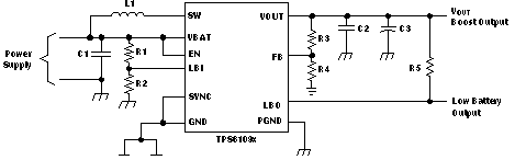 Figure 14. Typical Application Circuit for Adjustable Output Voltage Option Schematic
10.2.1.1 Design Requirements
Table 3. TPS6109x 5 V Output Design Parameters
| DESIGN PARAMETERS | TYPICAL VALUES |
|---|---|
| Input Voltage Range | 1.8 V to 5.0 V |
| Output Voltage | 5.0 V |
| Output Voltage Ripple | ±3% VOUT |
| Transient Response | ±10% VOUT |
| Input Voltage Ripple | ±200 mV |
| Output Current Rating | 500 mA |
| Operating Frequency | 600 kHz |
10.2.1.2 Detailed Design Procedure
The TPS6109x DC-DC converters are intended for systems powered by a dual or triple cell NiCd or NiMH battery with a typical terminal voltage between 1.8 V and 5.5 V. They can also be used in systems powered by one-cell Li-Ion with a typical stack voltage between 2.5 V and 4.2 V. Additionally, two or three primary and secondary alkaline battery cells can be the power source in systems where the TPS6109x is used.
10.2.1.2.1 Programming the Output Voltage
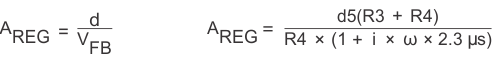
The output voltage of the TPS61090 DC-DC converter section can be adjusted with an external resistor divider. The typical value of the voltage on the FB pin is 500 mV. The maximum allowed value for the output voltage is 5.5 V. The current through the resistive divider should be about 100 times greater than the current into the FB pin. The typical current into the FB pin is 0.01 µA, and the voltage across R4 is typically 500 mV. Based on those two values, the recommended value for R4 should be lower than 500 kΩ, in order to set the divider current at 1 µA or higher. Because of internal compensation circuitry the value for this resistor should be in the range of 200 kΩ. From that, the value of resistor R3, depending on the needed output voltage (VO), can be calculated using Equation 1:
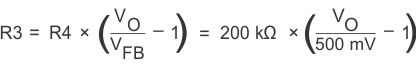
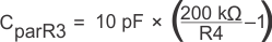
If as an example, an output voltage of 5.0 V is needed, a 1.8-MΩ resistor should be chosen for R3. If for any reason the value for R4 is chosen significantly lower than 200 kΩ additional capacitance in parallel to R3 is recommended. The required capacitance value can be easily calculated using Equation 2
10.2.1.2.2 Programming the LBI/LBO Threshold Voltage
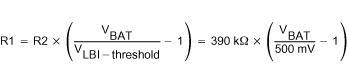
The current through the resistive divider should be about 100 times greater than the current into the LBI pin. The typical current into the LBI pin is 0.01 µA, and the voltage across R2 is equal to the LBI voltage threshold that is generated on-chip, which has a value of 500 mV. The recommended value for R2is therefore in the range of 500 kΩ. From that, the value of resistor R1, depending on the desired minimum battery voltage VBAT, can be calculated using Equation 3.
The output of the low battery supervisor is a simple open-drain output that goes active low if the dedicated battery voltage drops below the programmed threshold voltage on LBI. The output requires a pullup resistor with a recommended value of 1 MΩ. The maximum voltage which is used to pull up the LBO outputs should not exceed the output voltage of the DC-DC converter. If not used, the LBO pin can be left floating or tied to GND.
10.2.1.2.3 Inductor Selection
A boost converter normally requires two main passive components for storing energy during the conversion. A boost inductor and a storage capacitor at the output are required. To select the boost inductor, it is recommended to keep the possible peak inductor current below the current limit threshold of the power switch in the chosen configuration. For example, the current limit threshold of the TPS6109x's switch is 2500 mA at an output voltage of 5 V. The highest peak current through the inductor and the switch depends on the output load, the input (VBAT), and the output voltage (VOUT). Estimation of the maximum average inductor current can be done using Equation 4:
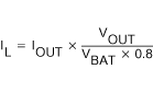
For example, for an output current of 500 mA at 5 V, at least 1750 mA of average current flows through the inductor at a minimum input voltage of 1.8 V.
The second parameter for choosing the inductor is the desired current ripple in the inductor. Normally, it is advisable to work with a ripple of less than 20% of the average inductor current. A smaller ripple reduces the magnetic hysteresis losses in the inductor, as well as output voltage ripple and EMI. But in the same way, regulation time at load changes rises. In addition, a larger inductor increases the total system costs. With those parameters, it is possible to calculate the value for the inductor by using Equation 5:
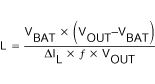
Parameter f is the switching frequency and ΔIL is the ripple current in the inductor, i.e., 20% × IL. In this example, the desired inductor has the value of 5.5 µH. With this calculated value and the calculated currents, it is possible to choose a suitable inductor. Care has to be taken that load transients and losses in the circuit can lead to higher currents as estimated in equation 4. Also, the losses in the inductor caused by magnetic hysteresis losses and copper losses are a major parameter for total circuit efficiency.
The following inductor series from different suppliers have been used with the TPS6109x converters:
Table 4. List of Inductors
| VENDOR | INDUCTOR SERIES |
|---|---|
| Sumida | CDRH6D28 |
| CDRH6D38 | |
| CDRH103R | |
| Wurth Elektronik | WE-PD type L |
| WE-PD type XL | |
| EPCOS | B82464G |
10.2.1.2.4 Capacitor Selection
10.2.1.2.4.1 Input Capacitor
At least a 10-µF input capacitor is recommended to improve transient behavior of the regulator and EMI behavior of the total power supply circuit. A ceramic capacitor or a tantalum capacitor with a 100-nF ceramic capacitor in parallel, placed close to the IC, is recommended.
10.2.1.2.4.2 Output Capacitor DC-DC Converter
The major parameter necessary to define the minimum value of the output capacitor is the maximum allowed output voltage ripple in steady state operation of the converter. This ripple is determined by two parameters of the capacitor, the capacitance and the ESR. It is possible to calculate the minimum capacitance needed for the defined ripple, supposing that the ESR is zero, by using equation Equation 6:
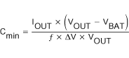
Parameter f is the switching frequency and ΔV is the maximum allowed ripple.
With a chosen ripple voltage of 10 mV, a minimum capacitance of 53 µF is needed. The total ripple is larger due to the ESR of the output capacitor. This additional component of the ripple can be calculated using Equation 7:
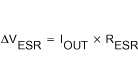
An additional ripple of 40 mV is the result of using a tantalum capacitor with a low ESR of 80 mΩ. The total ripple is the sum of the ripple caused by the capacitance and the ripple caused by the ESR of the capacitor. In this example, the total ripple is 50 mV. Additional ripple is caused by load transients. This means that the output capacitance needs to be larger than calculated above to meet the total ripple requirements. The output capacitor has to completely supply the load during the charging phase of the inductor. A reasonable value of the output capacitance depends on the speed of the load transients and the load current during the load change. With the calculated minimum value of 53 µF and load transient considerations, a reasonable output capacitance value is in a 100 µF range. For economical reasons this usually is a tantalum capacitor. Because of this the control loop has been optimized for using output capacitors with an ESR of above 30 mΩ.
10.2.1.2.4.3 Small Signal Stability
When using output capacitors with lower ESR, like ceramics, it is recommended to use the adjustable voltage version. The missing ESR can be easily compensated there in the feedback divider. Typically a capacitor in the range of 10 pF in parallel to R3 helps to obtain small signal stability with lowest ESR output capacitors. For more detailed analysis the small signal transfer function of the error amplifier and regulator, which is given is Equation 8, can be used.
10.2.1.3 Application Curves
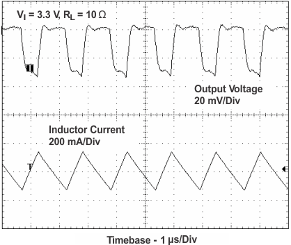 Figure 15. Output Voltage in Continuous Mode
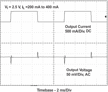 Figure 17. Load Transient Response
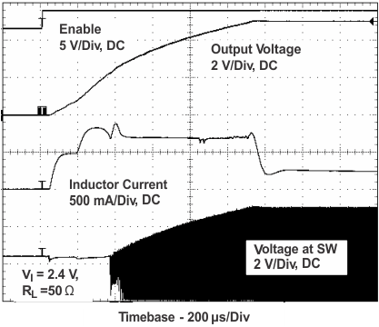 Figure 19. DC-DC Converter Start-Up After Enable
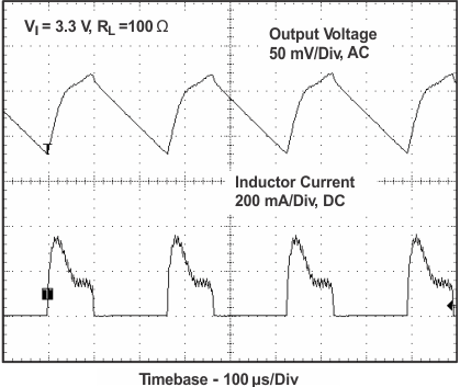 Figure 16. Output Voltage in Power Save Mode
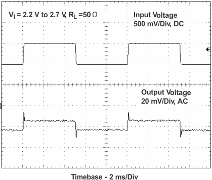 Figure 18. Line Transient Response
10.2.2 TPS6109x Application Schematic of 5 Vout With Maximum Output Power
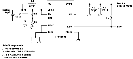 Figure 20. Power Supply Solution for Maximum Output Power Schematic
10.2.3 TPS6109x Application Schematic of 5 Vout and Auxiliary 10 Vout With Charge Pump
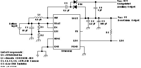 Figure 21. Power Supply Solution With Auxiliary Positive Output Voltage Schematic
10.2.4 TPS6109x Application Schematic of 5 Vout and Auxiliary -5 Vout With Charge Pump
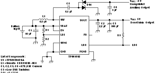 Figure 22. Power Supply Solution With Auxiliary Negative Output Voltage Schematic