SLVSAX2B September   2011  – June 2020 TPS61170-Q1

PRODUCTION DATA.  

  1. Features
  2. Applications
  3. Description
    1.     Device Images
      1.      Typical Application
  4. Revision History
  5. Pin Configuration and Functions
    1.     Pin Functions
  6. Specifications
    1. 6.1 Absolute Maximum Ratings
    2. 6.2 ESD Ratings
    3. 6.3 Recommended Operating Conditions
    4. 6.4 Thermal Information
    5. 6.5 Electrical Characteristics
    6. 6.6 Switching Characteristics
    7. 6.7 Typical Characteristics
  7. Detailed Description
    1. 7.1 Overview
    2. 7.2 Functional Block Diagram
    3. 7.3 Feature Description
      1. 7.3.1 Soft Start-up
      2. 7.3.2 Overcurrent Protection
      3. 7.3.3 Undervoltage Lockout
      4. 7.3.4 Thermal Shutdown
      5. 7.3.5 Enable and Shutdown
    4. 7.4 Device Functional Modes
      1. 7.4.1 PWM Program Mode
      2. 7.4.2 1-Wire Program Mode
      3. 7.4.3 EasyScale
    5. 7.5 Programming
      1. 7.5.1 Feedback Reference Program Mode Selection
  8. Application and Implementation
    1. 8.1 Application Information
    2. 8.2 Typical Applications
      1. 8.2.1 12-V to 24-V DC-DC Power Conversion
        1. 8.2.1.1 Design Requirements
        2. 8.2.1.2 Detailed Design Procedure
          1. 8.2.1.2.1 Program Output Voltage
          2. 8.2.1.2.2 Maximum Output Current
          3. 8.2.1.2.3 Switch Duty Cycle
          4. 8.2.1.2.4 Inductor Selection
          5. 8.2.1.2.5 Schottky Diode Selection
          6. 8.2.1.2.6 Compensation Capacitor Selection
          7. 8.2.1.2.7 Input and Output Capacitor Selection
        3. 8.2.1.3 Application Curve
      2. 8.2.2 5-V to 12-V DC-DC Power Conversion With Programmable Feedback Reference Voltage
      3. 8.2.3 12-V SEPIC (Buck-Boost) Converter
  9. Power Supply Recommendations
  10. 10Layout
    1. 10.1 Layout Guidelines
    2. 10.2 Layout Example
    3. 10.3 Thermal Considerations
  11. 11Device and Documentation Support
    1. 11.1 Device Support
      1. 11.1.1 Third-Party Products Disclaimer
    2. 11.2 Documentation Support
      1. 11.2.1 Related Documentation
    3. 11.3 Support Resources
    4. 11.4 Trademarks
    5. 11.5 Electrostatic Discharge Caution
    6. 11.6 Glossary
  12. 12Mechanical, Packaging, and Orderable Information

Typical Characteristics

L = TOKO A915_Y-100M, D1 = ONsemi MBR0540T1, unless otherwise noted

Table 1. Table of Graphs

FIGURE
Efficiency VIN = 5V; VOUT = 12 V, 18 V, 24 V, 30 V Figure 17
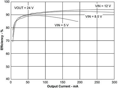
Efficiency VIN = 5 V, 8.5 V, 12 V; VOUT = 24 V Figure 1
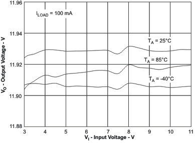
Output voltage accuracy ILOAD= 100 mA Figure 2
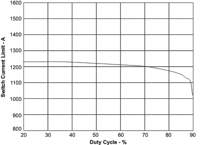
Switch current limit TA = 25°C Figure 3
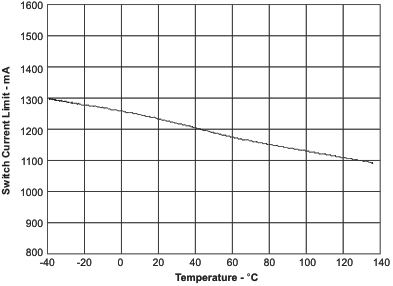
Switch current limit Figure 4
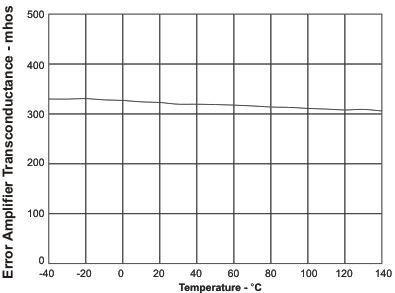
Error amplifier transconductance Figure 5
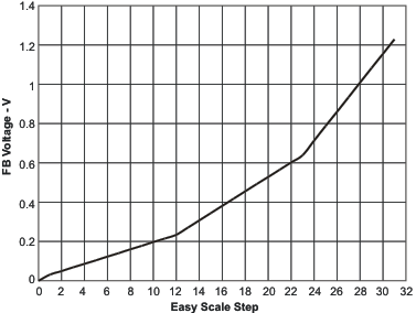
EasyScale step Figure 6
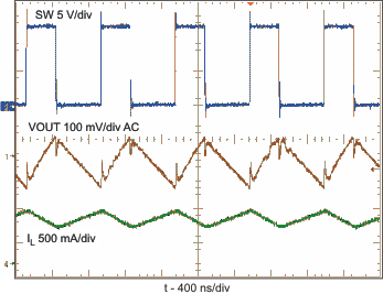
PWM switching operation VIN = 5 V; VOUT = 12 V; ILOAD= 250 mA Figure 7
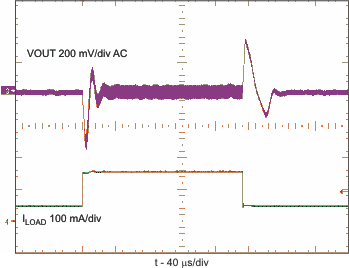
Load transient response VIN = 5 V; VOUT = 12 V; ILOAD= 50 mA to 150 mA Figure 8
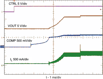
Start-up VIN = 5 V; VOUT = 12 V; ILOAD= 250 mA Figure 9
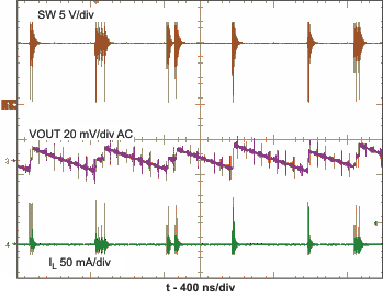
Skip-cycle switching VIN = 9 V ; VOUT = 12 V, ILOAD= 100 μA Figure 10
TPS61170-Q1 eff2_io_lvs789.gif
Figure 1. Efficiency vs Output Current
TPS61170-Q1 swc_dc_lvs789.gif
Figure 3. Switch Current Limit vs Duty Cycle
TPS61170-Q1 error_ta_lvs789.gif
Figure 5. Error Amplifier Transconductance vs Temperature
TPS61170-Q1 pwm_sw_lvs789.gif
Figure 7. PWM Switching Operation
TPS61170-Q1 startup_lvs789.gif
Figure 9. Start-Up
TPS61170-Q1 vo_vi_lvs789.gif
Figure 2. Output Voltage vs Input Voltage
TPS61170-Q1 swc_ta_lvs789.gif
Figure 4. Switch Current Limit vs Temperature
TPS61170-Q1 fbv_scale_lvs789.gif
Figure 6. FB Voltage vs EasyScale Step
TPS61170-Q1 ld_trans_lvs789.gif
Figure 8. Load Transient Response
TPS61170-Q1 skip_cyc_lvs789.gif
Figure 10. Skip-Cycle Switching