SLVSF65A December 2020 – May 2021 TPS92633-Q1
PRODUCTION DATA
- 1 Features
- 2 Applications
- 3 Description
- 4 Revision History
- 5 Pin Configuration and Functions
- 6 Specifications
-
7 Detailed Description
- 7.1 Overview
- 7.2 Functional Block Diagram
- 7.3
Feature Description
- 7.3.1 Power Supply (SUPPLY)
- 7.3.2 Enable and Shutdown (EN)
- 7.3.3 Reference Current (IREF)
- 7.3.4 Constant-Current Output and Setting (INx)
- 7.3.5 Analog Current Control (ICTRL)
- 7.3.6 Thermal Sharing Resistor (OUTx and RESx)
- 7.3.7 PWM Control (PWMx)
- 7.3.8 Supply Control
- 7.3.9
Diagnostics
- 7.3.9.1 IREF Short-to-GND Detection
- 7.3.9.2 IREF Open Detection
- 7.3.9.3 LED Short-to-GND Detection
- 7.3.9.4 LED Open-Circuit Detection
- 7.3.9.5 Single LED Short-Circuit Detection (SLS_REF)
- 7.3.9.6 LED Open-Circuit and Single LED Short-Circuit Detection Enable (DIAGEN)
- 7.3.9.7 Low Dropout Operation
- 7.3.9.8 Over-Temperature Protection
- 7.3.10 FAULT Bus Output With One-Fails–All-Fail
- 7.3.11 FAULT Table
- 7.3.12 LED Fault Summary
- 7.3.13 IO Pins Inner Connection
- 7.4 Device Functional Modes
- 8 Application and Implementation
- 9 Power Supply Recommendations
- 10Layout
- 11Device and Documentation Support
- 12Mechanical, Packaging, and Orderable Information
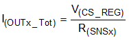
7.3.4 Constant-Current Output and Setting (INx)
The TPS92633-Q1 device is a high-side current driver for driving LEDs. The device controls each output current through regulating the voltage drop on an external high-side current-sense resistor, R(SNSx) between SUPPLY and INx independently for each channel. An integrated error amplifier drives an internal power transistor to maintain the voltage drop on the current-sense resistor R(SNSx) to V(CS_REG), therefore regulates the current output to target value. When the output current is in regulation, the current value for each channel can be calculated by using Equation 2.
where
- V(CS_REG) is variable according to Equation 3
- x = 1, 2 or 3 for output channel 1, 2 or 3
When the supply voltage drops below total LED string forward voltage plus required headroom voltage, the sum of V(DROPOUT) and V(CS_REG), the TPS92633-Q1 is not able to deliver enough current output as set by the value of R(SNSx), and the voltage across the current-sense resistor R(SNSx) is less than V(CS_REG).