SLVSF65A December 2020 – May 2021 TPS92633-Q1
PRODUCTION DATA
- 1 Features
- 2 Applications
- 3 Description
- 4 Revision History
- 5 Pin Configuration and Functions
- 6 Specifications
-
7 Detailed Description
- 7.1 Overview
- 7.2 Functional Block Diagram
- 7.3
Feature Description
- 7.3.1 Power Supply (SUPPLY)
- 7.3.2 Enable and Shutdown (EN)
- 7.3.3 Reference Current (IREF)
- 7.3.4 Constant-Current Output and Setting (INx)
- 7.3.5 Analog Current Control (ICTRL)
- 7.3.6 Thermal Sharing Resistor (OUTx and RESx)
- 7.3.7 PWM Control (PWMx)
- 7.3.8 Supply Control
- 7.3.9
Diagnostics
- 7.3.9.1 IREF Short-to-GND Detection
- 7.3.9.2 IREF Open Detection
- 7.3.9.3 LED Short-to-GND Detection
- 7.3.9.4 LED Open-Circuit Detection
- 7.3.9.5 Single LED Short-Circuit Detection (SLS_REF)
- 7.3.9.6 LED Open-Circuit and Single LED Short-Circuit Detection Enable (DIAGEN)
- 7.3.9.7 Low Dropout Operation
- 7.3.9.8 Over-Temperature Protection
- 7.3.10 FAULT Bus Output With One-Fails–All-Fail
- 7.3.11 FAULT Table
- 7.3.12 LED Fault Summary
- 7.3.13 IO Pins Inner Connection
- 7.4 Device Functional Modes
- 8 Application and Implementation
- 9 Power Supply Recommendations
- 10Layout
- 11Device and Documentation Support
- 12Mechanical, Packaging, and Orderable Information
3 Description
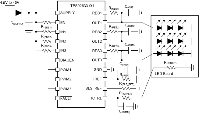
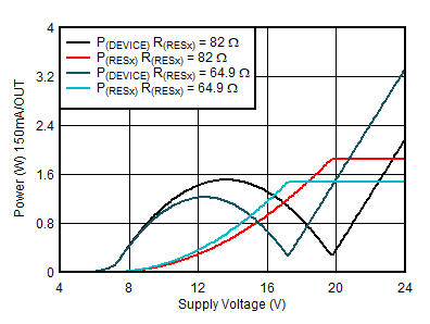
The TPS92633-Q1 three-channel LED driver includes an unique thermal management design to reduce temperature rising on the device. The TPS92633-Q1 is a linear driver directly powered by automotive batteries with large voltage variations to output full current loads up to 150 mA per channel. External shunt resistors are leveraged to share output current and dissipate power out of the driver. The TPS92633-Q1 also drives LED units and off-board brightness binning resistors to simplify the manufacturing process and lower whole system cost. Its full-diagnostic capabilities include LED open, LED short-to-GND circuit and single LED short circuit detection.
The one-fails-all-fail feature of TPS92633-Q1 is able to work together with other LED drivers, such as the TPS9261x-Q1, TPS92630/8-Q1, and TPS92830-Q1 devices, to address different requirements.
| PART NUMBER | PACKAGE(1) | BODY SIZE (NOM) |
|---|---|---|
| TPS92633-Q1 | HTSSOP (20) | 6.50 mm × 4.40 mm |
 Typical Application Diagram
 Power Dissipation On Device