SLVSF65A December 2020 – May 2021 TPS92633-Q1
PRODUCTION DATA
- 1 Features
- 2 Applications
- 3 Description
- 4 Revision History
- 5 Pin Configuration and Functions
- 6 Specifications
-
7 Detailed Description
- 7.1 Overview
- 7.2 Functional Block Diagram
- 7.3
Feature Description
- 7.3.1 Power Supply (SUPPLY)
- 7.3.2 Enable and Shutdown (EN)
- 7.3.3 Reference Current (IREF)
- 7.3.4 Constant-Current Output and Setting (INx)
- 7.3.5 Analog Current Control (ICTRL)
- 7.3.6 Thermal Sharing Resistor (OUTx and RESx)
- 7.3.7 PWM Control (PWMx)
- 7.3.8 Supply Control
- 7.3.9
Diagnostics
- 7.3.9.1 IREF Short-to-GND Detection
- 7.3.9.2 IREF Open Detection
- 7.3.9.3 LED Short-to-GND Detection
- 7.3.9.4 LED Open-Circuit Detection
- 7.3.9.5 Single LED Short-Circuit Detection (SLS_REF)
- 7.3.9.6 LED Open-Circuit and Single LED Short-Circuit Detection Enable (DIAGEN)
- 7.3.9.7 Low Dropout Operation
- 7.3.9.8 Over-Temperature Protection
- 7.3.10 FAULT Bus Output With One-Fails–All-Fail
- 7.3.11 FAULT Table
- 7.3.12 LED Fault Summary
- 7.3.13 IO Pins Inner Connection
- 7.4 Device Functional Modes
- 8 Application and Implementation
- 9 Power Supply Recommendations
- 10Layout
- 11Device and Documentation Support
- 12Mechanical, Packaging, and Orderable Information
7.3.8 Supply Control
The TPS92633-Q1 can support supply control to turn ON and OFF output current. When the voltage applied on the SUPPLY pin is higher than the LED string forward voltage plus needed headroom voltage at required current, and the PWM pin voltage is high, the output current is turned ON and well regulated. However, when the voltage applied on the SUPPLY pin is lower than V(POR_falling), the output current is turned OFF. With this feature, the power supply voltage in designed pattern can control the output current ON/OFF. The brightness is adjustable if the ON/OFF frequency is fast enough. Because of the high accuracy design of PWM threshold in TPS92633-Q1, it enables a resistor divider on the PWM pin to set the SUPPLY threshold higher than LED forward voltage plus required headroom voltage as shown in Figure 7-6. The headroom voltage is basically the summation of V(DROPOUT) and V(CS_REG). When the voltage on the PWM pin is higher than VIH(PWM), the output current is turned ON. However, when the voltage on the PWM is lower than VIL(PWM), the output current is turned OFF. The SUPPLY threshold voltage can be calculated by using Equation 5.
 Figure 7-6 Application
Schematic For Supply Control LED Brightness
Figure 7-6 Application
Schematic For Supply Control LED Brightness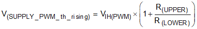
where
- VIH(PWM) = 1.26 V (maximum)