SLVSLY3 June   2026 SN74UVP1G07

ADVANCE INFORMATION  

  1.   1
  2. 1 Features
  3. 2 Applications
  4. 3 Description
  5. 4 Pin Configuration and Functions
  6. 5 Specifications
    1. 5.1 Absolute Maximum Ratings
    2. 5.2 ESD Ratings
    3. 5.3 Recommended Operating Conditions
    4. 5.4 Thermal Information
    5. 5.5 Electrical Characteristics
    6. 5.6 Switching Characteristics
  7. 6 Parameter Measurement Information
  8. 7 Detailed Description
    1. 7.1 Overview
    2. 7.2 Functional Block Diagram
    3. 7.3 Feature Description
    4. 7.4 Device Functional Modes
  9. 8 Application and Implementation
    1. 8.1 Application Information
    2. 8.2 Typical Application
      1. 8.2.1 Design Requirements
      2. 8.2.2 Detailed Design Procedure
    3. 8.3 Power Supply Recommendations
    4. 8.4 Layout
      1. 8.4.1 Layout Guidelines
      2. 8.4.2 Layout Example
  10. 9 Device and Documentation Support
    1. 9.1 Documentation Support
      1. 9.1.1 Related Documentation
    2. 9.2 Receiving Notification of Documentation Updates
    3. 9.3 Support Resources
    4. 9.4 Trademarks
    5. 9.5 Electrostatic Discharge Caution
    6. 9.6 Glossary
  11. 10Revision History
  12. 11Mechanical, Packaging, and Orderable Information
    1. 11.1 Tape and Reel Information
    2. 11.2 Mechanical Data

Pin Configuration and Functions

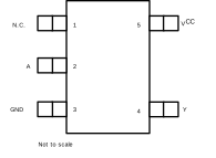
SN74UVP1G07 DBV or DCK Package,5-Pin SOT-23 or SC-70(Top View) Figure 4-1 DBV or DCK Package,
5-Pin SOT-23 or SC-70
(Top View)
SN74UVP1G07 DPW Package,5-Pin X2SON(Top View) Figure 4-2 DPW Package,
5-Pin X2SON
(Top View)
Table 4-1 Pin Functions
PIN TYPE(1) DESCRIPTION
NAME DBV,DCK, DTX DPW
N.C. 1 1 — Not internally connected
A 2 2 I
GND 3 3 G Ground pin
Y 4 4 O Output Y (open drain)
VCC 5 5 P Power pin
I = Input, O = Output, G = Ground, P = Power
SN74UVP1G07 DRY or DSF Package,5-Pin USON or X2SON(Top
                    View) Figure 4-3 DRY or DSF Package,
5-Pin USON or X2SON
(Top View)
Table 4-2 Pin Functions
PIN TYPE(1) DESCRIPTION
NAME DSF, DRY
N.C. 1, 5 — Not internally connected
A 2 I Input A
GND 3 G Ground pin
Y 4 O Output Y (open drain)
VCC 6 P Power pin
I = Input, O = Output, G = Ground, P = Power