SLVU189B february   2007  – may 2023 TPS74701 , TPS74801


  1.   1
  2.   Abstract
  3.   Trademarks
  4. 1Introduction
    1. 1.1 Performance Specification Summary
    2. 1.2 Modifications
  5. 2Input and Output Connector Descriptions
    1. 2.1  J1–VIN/GND
    2. 2.2  J2–GND
    3. 2.3  J3–VIN
    4. 2.4  J4–VBIAS
    5. 2.5  J5–GND
    6. 2.6  J6–VOUT
    7. 2.7  J7–GND
    8. 2.8  J8–VOUT/GND
    9. 2.9  J10–EN
    10. 2.10 J11–GND
    11. 2.11 J12-VIN/GND
    12. 2.12 J13-VOUT/GND
    13. 2.13 JP1–1 ms/Simult Versus 10 ms/Ratio
    14. 2.14 S1
    15. 2.15 TP1
    16. 2.16 TP2
    17. 2.17 TP3
    18. 2.18 TP4
  6. 3Test Setup
  7. 4Test Results
  8. 5Board Layout
  9. 6Bill of Materials and Schematic
    1. 6.1 Schematic Drawing
  10. 7Revision History

Schematic Drawing

Figure 6-1 is the schematic for the TPS74x01EVM-177.
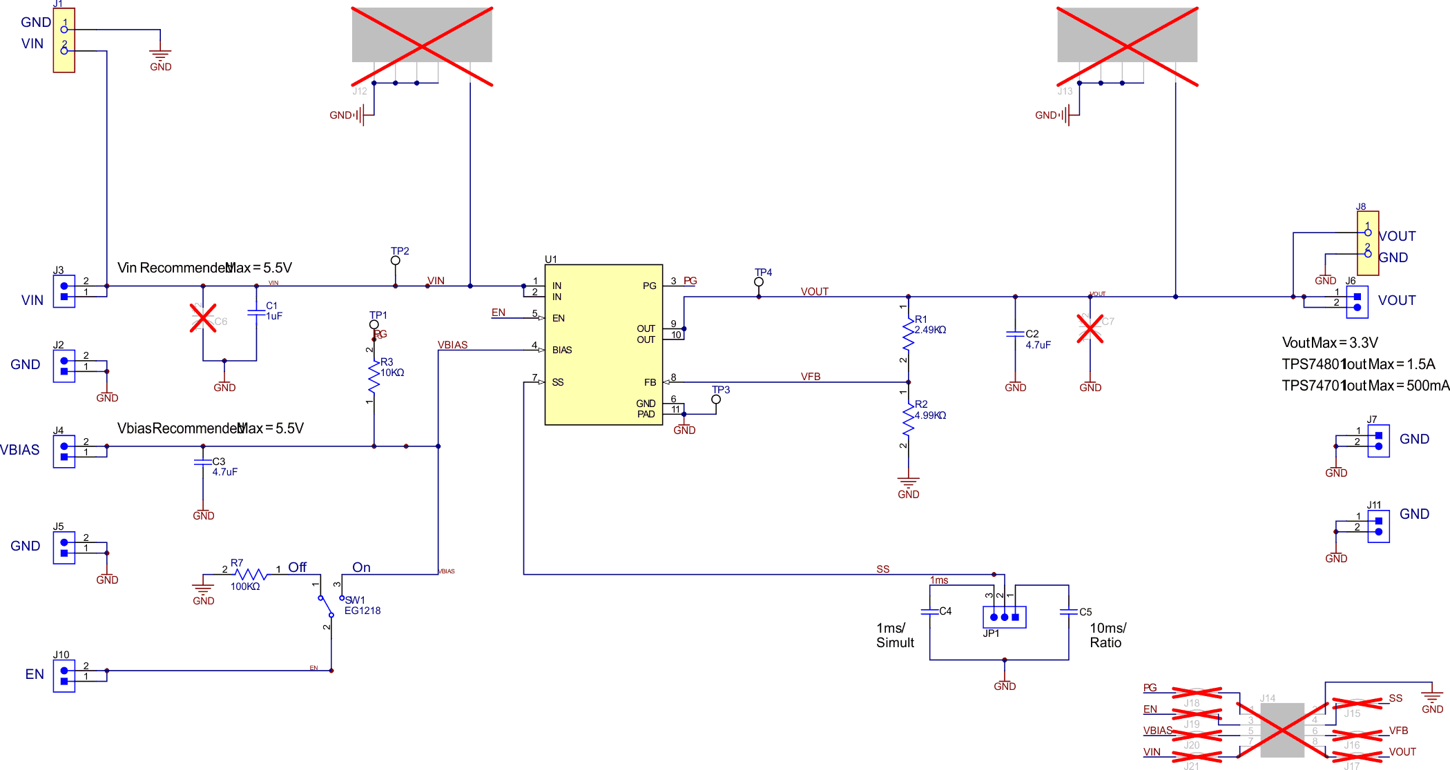
GUID-20230130-SS0I-CVJW-6N72-QNRCPP1M7DKL-low.gif Figure 6-1 Schematic