SLVUAX8B November 2016 – August 2021
- Trademarks
- 1Introduction
-
2Test Setup and Results
- 2.1 Input/Output Connections
- 2.2 Efficiency
- 2.3 Output Voltage Load Regulation
- 2.4 Output Voltage Line Regulation
- 2.5 Load Transients
- 2.6 Loop Characteristics
- 2.7 Output Voltage Ripple
- 2.8 Input Voltage Ripple
- 2.9 Powering Up
- 2.10 Powering Down
- 2.11 Start-Up Into Pre-Bias
- 2.12 Hiccup Mode Current Limit
- 3Board Layout
- 4Schematic and Bill of Materials
- 5Revision History
2.7 Output Voltage Ripple
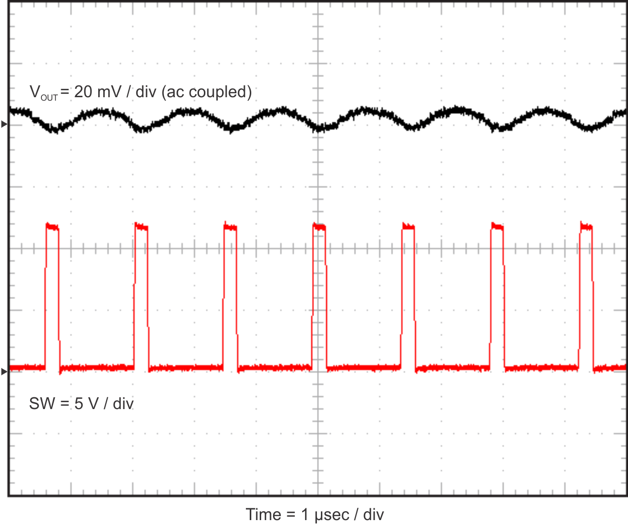
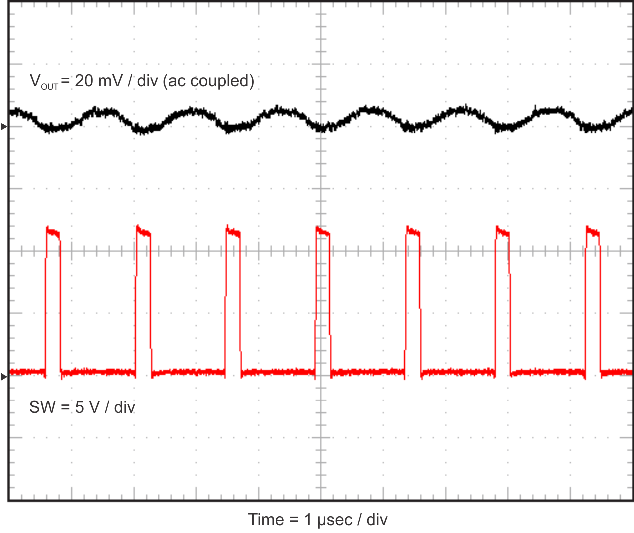
Figure 2-8 and Figure 2-9 show the TPS54824EVM-779 output voltage ripple. The load currents are no load and 8 A. VIN = 12 V. The ripple voltage is measured directly across TP9 and TP4.
 Figure 2-8 TPS54824EVM-779 Output Ripple, No Load
 Figure 2-9 TPS54824EVM-779 Output Ripple, 8-A Load