SLVUBI1 May 2021
4.6 Loop Frequency Response
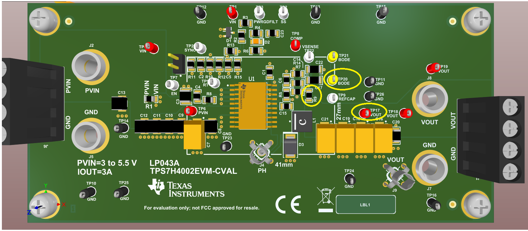
Measuring the frequency response of the feedback loop requires a unique test setup as well as physical changes to the EVM. The 0-Ω resistor jumper R9, just above the output inductor, L1, must be lifted to break the loop. Both test points TP20 (BODE) and TP15 (VOUT) are used for connections to the Bode100 instruments.
 Figure 4-7 EVM Modification to Measure
Frequency Response
Figure 4-7 EVM Modification to Measure
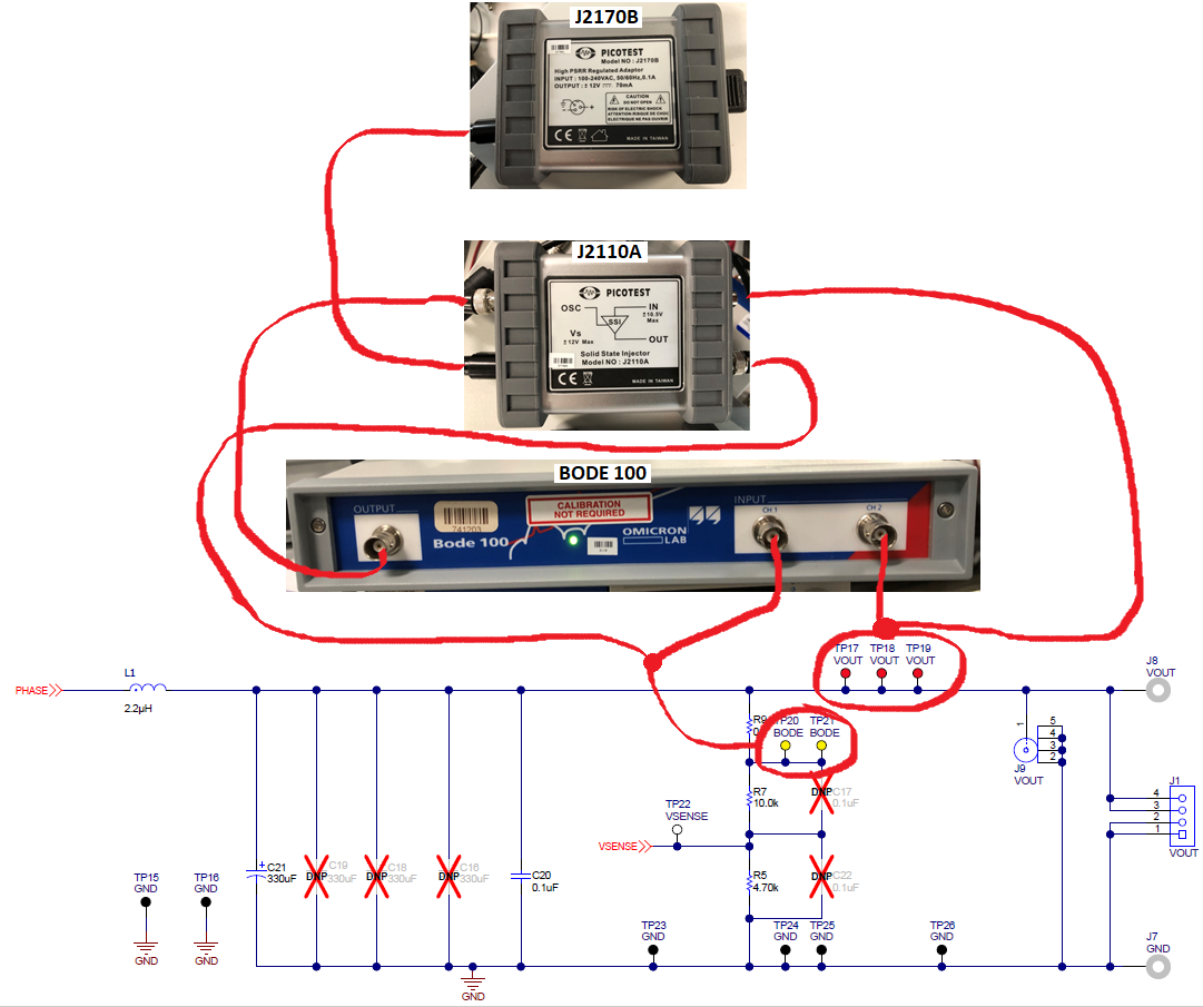
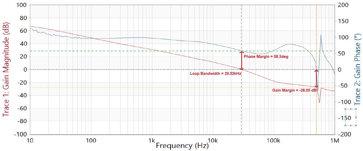
Frequency ResponseThe test setup which includes several connections to Picotest Bode100 test instruments is shown in Figure 4-8. Measurement results are shown in Figure 4-9 and in Figure 4-10. The CHF, high frequency pole, component of the compensation circuit is optional. Omitting it results in slightly increased phase margin. However, the benefit of including it is that the gain curve is set in a downward trajectory as frequency increases, making a monotonic gain curve more likely to be achieved.
 Figure 4-8 Frequency Response Test
Setup
 Figure 4-9 Frequency Response IOUT = 3
A
 Figure 4-10 Frequency Response IOUT = 0
A