SLVUBO4B March   2019  – September 2021 TPS55288


  1.   Trademarks
  2. 1Introduction
    1. 1.1 Performance Specification
    2. 1.2 Modification
      1. 1.2.1 Modification
  3. 2Connector, Test Point, and Jumper Descriptions
    1. 2.1 Connector and Test Point Descriptions
    2. 2.2 Jumper Configuration
      1. 2.2.1 JP1 (ENABLE)
      2. 2.2.2 JP2 and JP3 (External Feedback and Internal Feedback Selection)
      3. 2.2.3 JP4 (SYNC)
  4. 3Test Procedure
  5. 4Software User Interface
    1. 4.1 Install USB2ANY Explorer
    2. 4.2 GUI Installation
    3. 4.3 Interface Hardware Setup
    4. 4.4 User Interface Operation
    5. 4.5 Register Map Screen
  6. 5Schematic, Bill of Materials, and Board Layout
    1. 5.1 Schematic
    2. 5.2 Bill of Materials
    3. 5.3 Board Layout
  7. 6Revision History

Register Map Screen

The Register Map screen shows a register-wise view of all parameters. Here, single registers can be read or written to the device (if applicable). Refer to the TPS55288 36-V, 16-A Buck-Boost Converter with I2C Interface Data Sheet for a detailed description of the TPS55288 registers.
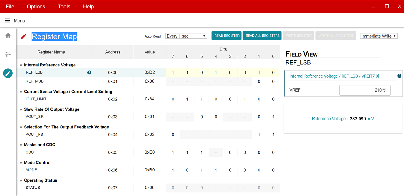
GUID-0A074E09-3033-4E3F-86D0-EBA2FB8F3A8A-low.pngFigure 4-7 GUI Register Map Screen