SLVUC27 January 2021 TPS61094
3.3 PCB Layouts
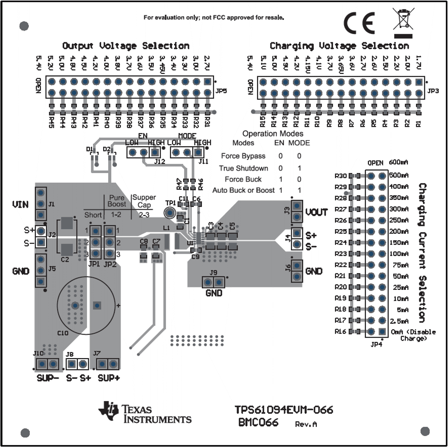
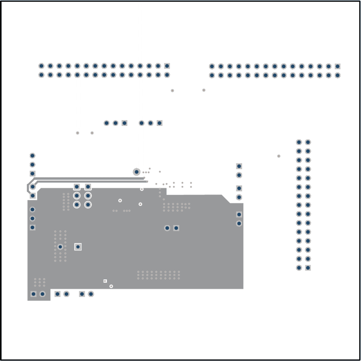
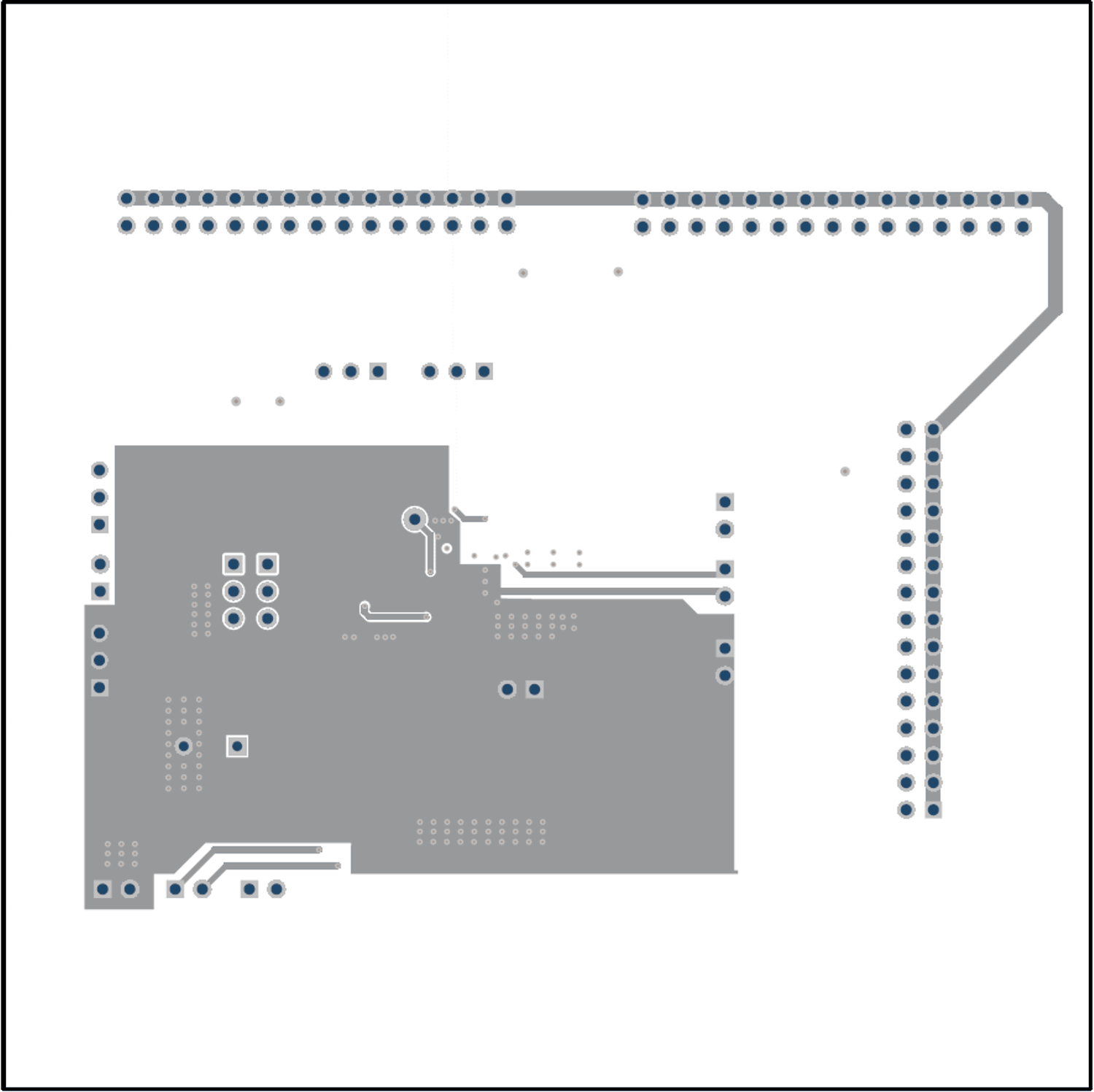
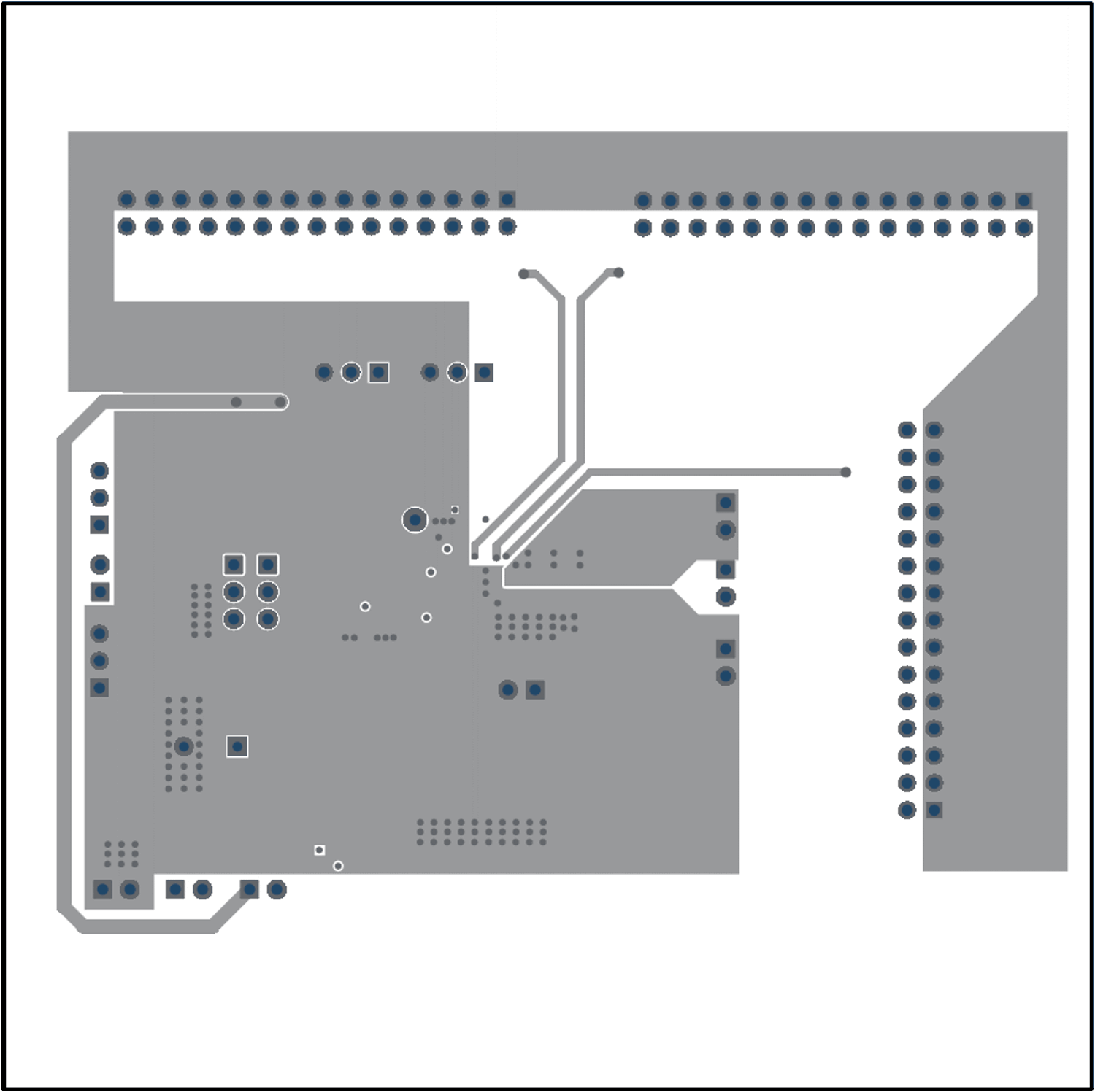
The TPS61094EVM board is a 4-layer PCB. The top and bottom layers copper thickness is 2-oz. The two inner layers copper thickness is 1-oz.Figure 3-2 and Figure 3-5 show the top view and bottom view, respectively. Figure 3-3 and Figure 3-4 show the inner layer 1 and inner layer 2, respectively.
 Figure 3-2 TPS61094EVM-066 Top-Side
Layout
 Figure 3-3 TPS61094EVM-066 Inner Layer1
Layout
 Figure 3-4 TPS61094EVM-066 Inner Layer2
Layout
 Figure 3-5 TPS61094EVM-066 Bottom Side
Layout