SLYY193C january 2023 – april 2023 LMQ61460-Q1 , TPS54319 , TPS62088 , TPS82671 , UCC12040 , UCC12050
- At a glance
- Authors
- 3
- What is power density?
- What limits power density?
- What limits power density: switching losses
- Key limiting factor No. 1: charge-related losses
- Key limiting factor No. 2: reverse-recovery losses
- Key limiting factor No. 3: turn-on and turn-off losses
- What limits power density: thermal performance
- How to break through power density barriers
- Switching loss innovations
- Package thermal innovations
- Advanced circuit design innovations
- Integration innovations
- Conclusion
- Additional resources
Advanced circuit design innovations
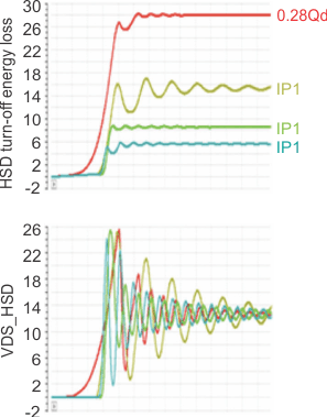
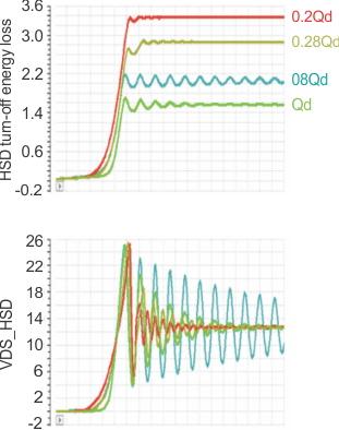
A negative byproduct of lower Rsp and lower RQ FoMs is the impact that a reduced drain charge has on transition losses. Looking at Figure 17, you can see that for a fixed amount of voltage overshoot, the turn-off loss of this buck converter goes up significantly as the drain charge reduces. In the presence of this trade-off, new and advanced gate driver intellectual property (IP) is necessary to switch the MOSFETs as fast as possible while keeping them inside their electrical safe operating area, despite a continued roadmap of improved RQ FoM MOSFETs. As the drain charge reduces, the turn-off energy increases in order to maintain a fixed drain-to-source voltage stress.
 Figure 17 Turn-off energy losses for
various MOSFET technologies.
Figure 17 Turn-off energy losses for
various MOSFET technologies.Along these lines, TI has recently developed a family of gate-driver techniques that enables very fast switching despite the lower RQ FoM MOSFETs, resulting in better charge and transition losses but still keeping the MOSFETs in their electrical safe operating area. As you can see when comparing Figure 18 and Figure 19, it is possible to reduce the turn-off energy loss by as much as 79% while keeping the peak voltage stress fixed. In some designs, as shown in Figure 19, this reduction can result in efficiency gains as high as 4% at the peak efficiency point.
 Figure 18 Comparison of gate-driver IP
that enables low drain charge and low turn-off energy.
 Figure 19 Impact of gate-driver IP on
system efficiency.
Figure 19 Impact of gate-driver IP on
system efficiency.In addition to advanced gate-driver technology, there is significant opportunity to improve power density through topology innovations. Figure 20 illustrates a flying capacitor four-level (FC4L) converter topology that enables a number of critical power density advantages, including better device FoMs through lower device voltage ratings, reduced magnetic filter sizes and better thermal distribution. These benefits translate into the improved power density shown in Figure 21. Compared to other topologies using SiC, the TI solution offers a significant volume reduction through the use of this particular topology, combined with GaN benefits and advanced packaging technologies. The FC4L GaN solution from TI offers the best power density.
 Figure 20 Flying capacitor four-level
converter topology using GaN switches.
 Figure 21 Overall volume of topologies
and switch types.