SLYY193C january 2023 – april 2023 LMQ61460-Q1 , TPS54319 , TPS62088 , TPS82671 , UCC12040 , UCC12050
- At a glance
- Authors
- 3
- What is power density?
- What limits power density?
- What limits power density: switching losses
- Key limiting factor No. 1: charge-related losses
- Key limiting factor No. 2: reverse-recovery losses
- Key limiting factor No. 3: turn-on and turn-off losses
- What limits power density: thermal performance
- How to break through power density barriers
- Switching loss innovations
- Package thermal innovations
- Advanced circuit design innovations
- Integration innovations
- Conclusion
- Additional resources
Package thermal innovations
The ability to get the heat out of an integrated circuit (IC) package directly impacts power density. As mentioned previously, this becomes an increasingly important problem as packages continue to shrink. Further, in a typical power converter, the semiconductor devices can often become the hottest part of the solution, especially with the Rsp shrinking rapidly.
TI has invested in the development and adoption of the HotRod™ package, which replaces typical bond-wire type quad flat no-lead packages (QFNs) with a flip-chip style package. Figure 9 and Figure 10 show how a HotRod QFN can eliminate the bond wires while keeping a QFN-like footprint. This results in a significant reduction in parasitic loop inductance, typical in flip-chip packages, while also keeping some of the benefits of the QFN package thermal performance. The HotRod QFN includes an interconnect between the leadframe and die.
 Figure 9 Standard bond-wire QFN package
with exposed pad.
 Figure 10 HotRod interconnect package
(flip-chip-on-lead) QFN package.
 One challenge with the HotRod package is that it becomes more difficult to build large die attach pads (DAPs), which are typically very helpful in improving package thermals. To overcome this challenge, TI recently enhanced the HotRod QFN to maintain its existing advantages while simultaneously enabling packages with large DAPs.
Figure 11, Figure 12 and Figure 14 show the 4-A LM60440 synchronous converter that includes these technology enhancements to improve thermal performance. You can see that the footprint is conducive to a large DAP in the center of the package. This DAP has about a 15% temperature rise benefit compared to the previous generation. You can read more about the evolution of these packages in our Analog Design Journal article, Designing with small DC/DC converters: HotRod™ QFN vs. Enhanced HotRod™ QFN Packaging.
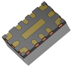 Figure 11 Enhanced HotRod QFN with a
large DAP.
  Figure 12 Pinout of LM60440 in Enhanced
HotRod QFN.
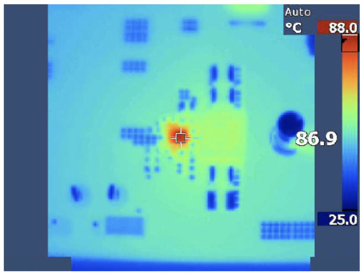 Figure 13 Thermal performance of a
conventional HotRod package.
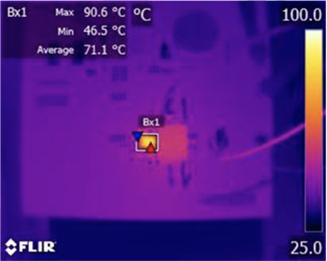 Figure 14 Thermal performance of the
LM60440 with DAP in the Enhanced HotRod QFN package, with average temperature
lowered to 71.1°C.
 Additionally, many designers prefer to leverage small-outline transistor (SOT) surface-mount packages, as they tend to be low cost and their pin leads are easier to assemble with. TI has paired improved process technology and circuit IP with the SOT-563 package so that the low-profile, dual-row pin configuration can meet the demands for higher current density. The TPS566242 3-V to 16-V synchronous buck converter is one recent example. The device supports up to 6 A of continuous current at 98% duty cycle in a 1.6-mm x 1.6-mm SOT-563 (6-pin) footprint.
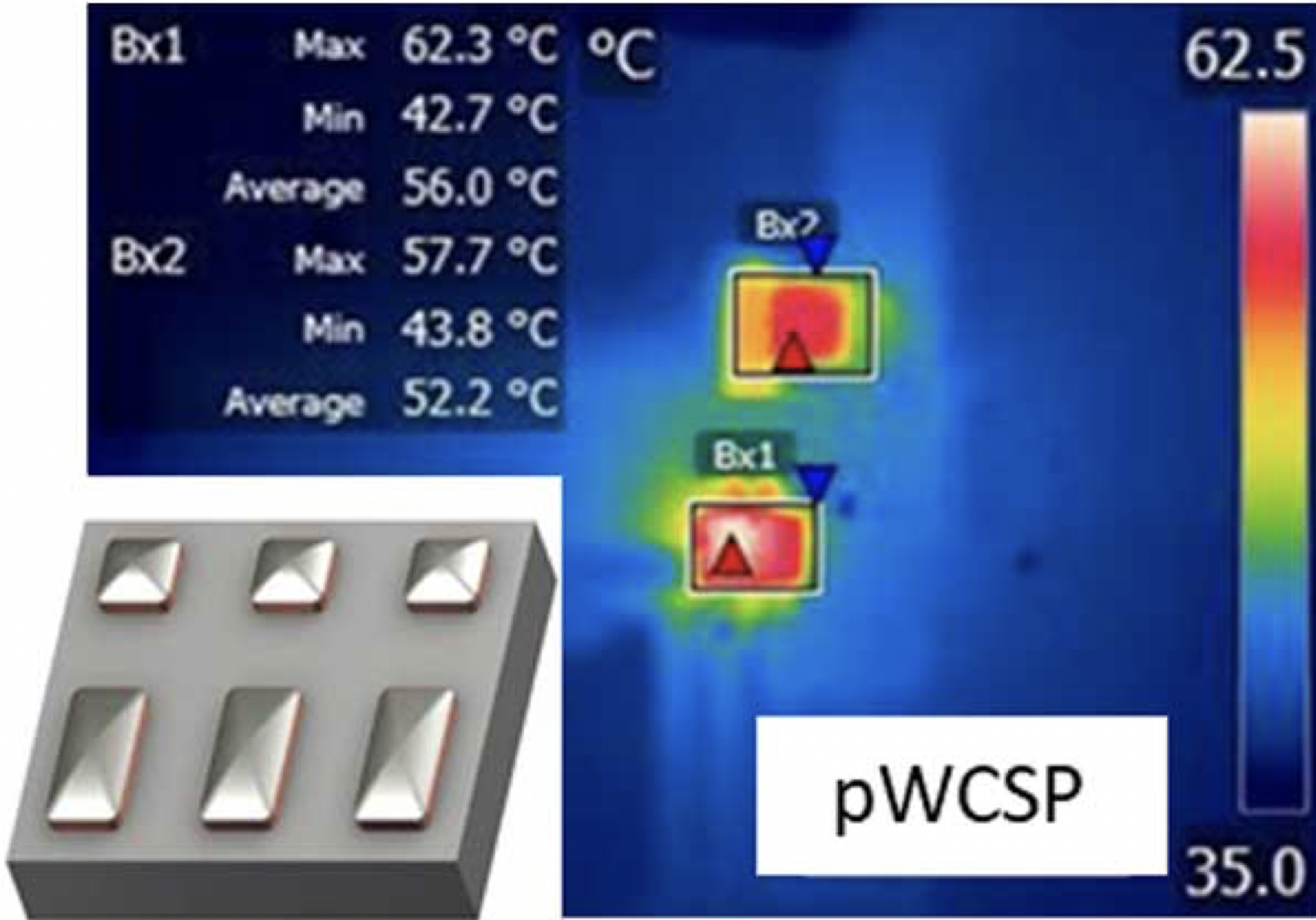
Similarly, when working with wafer chip-scale packages (WCSPs), most of the heat conducts directly out of the bumps, down to the PCB. The larger the bump area in a WCSP, the better the thermal performance. TI recently developed and released PowerCSP™ packaging, which aims to improve package thermals and electrical performance by replacing some of the typical circular bumps in a WCSP with large solder bars. Figure 15 illustrates an example implementation of this technology in the TPS62088. Figure 15 shows the standard WCSP, while Figure 16 shows the same device with the PowerCSP packaging. The temperature rise is reduced by about 5% without any other changes in the system.
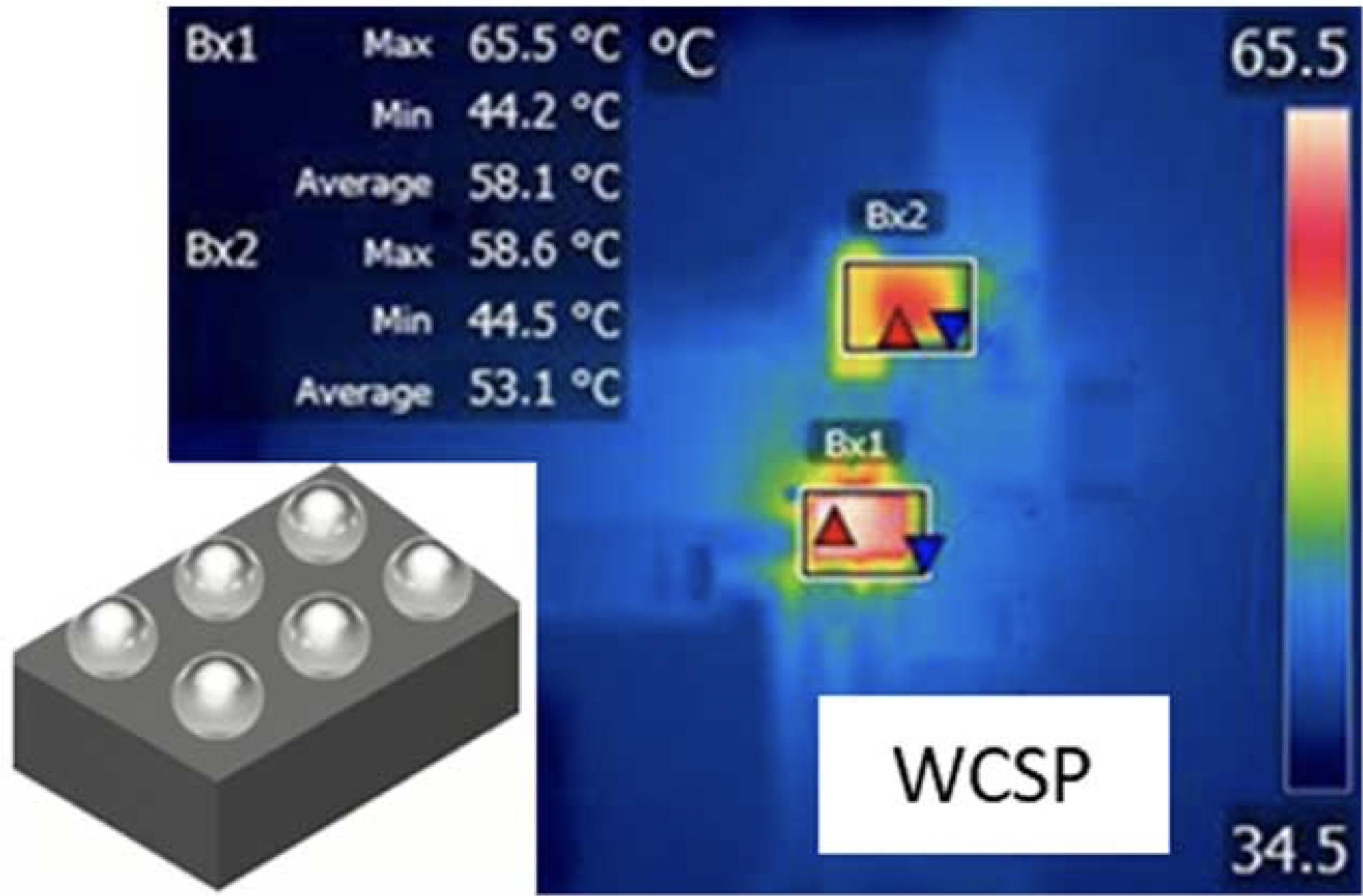
| VIN = 5 V | VOUT = 1.8 V |
| IOUT = 3 A | TA = 25°C |
| Measurement point: Bx1 |
| VIN = 5 V | VOUT = 1.8 V |
| IOUT = 3 A | TA = 25°C |
| Measurement point: Bx1 |