SLYY193C january 2023 – april 2023 LMQ61460-Q1 , TPS54319 , TPS62088 , TPS82671 , UCC12040 , UCC12050
- At a glance
- Authors
- 3
- What is power density?
- What limits power density?
- What limits power density: switching losses
- Key limiting factor No. 1: charge-related losses
- Key limiting factor No. 2: reverse-recovery losses
- Key limiting factor No. 3: turn-on and turn-off losses
- What limits power density: thermal performance
- How to break through power density barriers
- Switching loss innovations
- Package thermal innovations
- Advanced circuit design innovations
- Integration innovations
- Conclusion
- Additional resources
What limits power density?
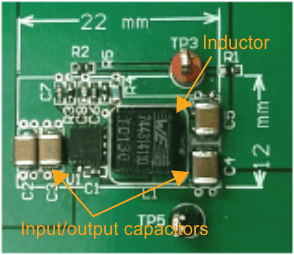
Engineers and researchers have focused on trying to find ways to improve power density for years. It is a challenging task. Most have focused their efforts on reducing the size of passive components used for energy conversion. Inductors, capacitors, transformers and heat sinks typically take up the largest portion of the power solution size, as shown in Figure 4. The semiconductor switches and control circuitry are considerably smaller and more integrated.
 Figure 4 Passive components such as inductors and capacitors can take up considerable space.
How do you reduce the size of passive components? One simple solution is to increase the switching frequency. The passive components in switching converters store and release energy every switching cycle. Higher switching frequencies require less energy storage for each of those cycles. For example, consider Equation 1, the design equation for the inductor in a buck converter:
where
- L is the inductance
- D is the duty ratio
- ΔIL is the inductor current ripple
- fSW is the switching frequency
- VL is voltage across the inductor
The inductance needed (L) is inversely proportional to switching frequency (fSW). As the switching frequency increases, the inductance decreases. Lower inductance leads to smaller inductors and space savings. Figure 5 illustrates the difference in size for the inductors needed in a 3-A, 36-V converter switching at 400 kHz versus 2 MHz.
 Figure 5 Size comparison of a 3-A, 36-V converter switching at 400 kHz (left) and 2 MHz (right).
There are other size benefits of higher switching frequencies. Increasing the switching frequency enables an increase in the control-loop bandwidth, which makes it possible to meet transient performance requirements with less output capacitance. You can design differential-mode electromagnetic interference (EMI) filters with less inductance and capacitance, and use smaller transformers without saturating the magnetic core material.
So why doesn’t everybody just increase the switching frequency? As it turns out, it is much easier said than done. Even if you shrunk down all of the passive elements used in power converters to an insignificant size, there would still be opportunities to reduce the power solution size. Power switches, gate drivers, mode-setting resistors, feedback network components, EMI filters, current-sensing components, interfacing circuits, heat sinks and many other components take up valuable real estate. All of these aspects of the overall power design are areas where innovation leads to improved power density. Let’s review the primary contributors that limit a designer’s ability to improve power density.