SLYY195A August 2020 – May 2022 BQ25790 , BQ25792 , BQ25798
Integrated components maximize power density
As described so far, the USB PD charging solution involves multiple external devices, including control units, MOSFETs and sensing resistors, which have not been optimized in terms of solution size and BOM cost.
The fully integrated buck-boost charger shown in Figure 2 can simplify the system-level design of a USB PD charging solution. First, the input current sensing is integrated into the charge. With this sensed input current, the charger provides the input current regulation and input overcurrent protection to avoid adapter overload. As part of the input overvoltage and overcurrent protection circuit, the control logic and driving circuitry for the external back-to-back MOSFETs are also integrated into the charger. These features make it possible to eliminate the unit that supports input power-path management and input current sensing from the block diagram.
Multiple input sources are a common trend in portable devices. For example, the input source could be a USB adapter, conventional barrel-jack adapter, charging case or solar power. The two drivers for the back-to-back MOSFETs enable the charger to select the input voltage from two different input sources.
The charger also integrates all four switching MOSFETs, the related control logic and the drivers. The battery FET to manage the NVDC power path is integrated inside the charger. By sensing the charging current flowing through the battery FET, you can eliminate the external sensing resistor at the charger’s output side.
Implementing the bidirectional operation of the four FETs’ buck-boost converter allows the charger to support OTG mode itself. When the adapter is present, the charger operates in forward charging mode with power flow from VBUS to the battery.
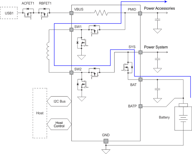
 Figure 3 USB Type-C™ FRS realized by
single buck-boost charger.
Figure 3 USB Type-C™ FRS realized by
single buck-boost charger.When the adapter is disconnected, the power flow reverses from the battery to VBUS. The OTG mode output voltage at VBUS covers the full USB PD voltage range, from 2.8 V to 22 V with a 10-mV programmable step size, which is compatible with the USB PD 3.0 specification.
In order to support FRS for the USB Type-C port, this integrated buck-boost charger implements a novel backup mode. In this context, backup mode refers to an ultra-fast transition for the buck-boost charger from forward charging mode to reverse OTG mode without the bus voltage crashing.
Looking at the application diagram in Figure 3, the adapter connects at the USB port, powering the system and charging the battery through the buck- boost power stage. At the same time, the adapter could power accessories from the charger’s PMID output. When the adapter is disconnected, the battery’s internal FET can still power the system; however, the accessories at PMID might lose power.
With backup mode enabled, the charger is able to monitor the VBUS voltage; the VBUS voltage dropping lower than the preset threshold indicates the adapter’s removal. Once it detects a removal, the charger shifts from forward charging mode to OTG mode with minimal delay time, discharges the battery to regulate the VBUS voltage, and achieves FRS by itself. When the adapter is unplugged, the sources to power the system and accessories can switch from the adapter to the battery seamlessly, making it possible to eliminate the DC/DC converter for OTG mode and FRS from the block diagram.
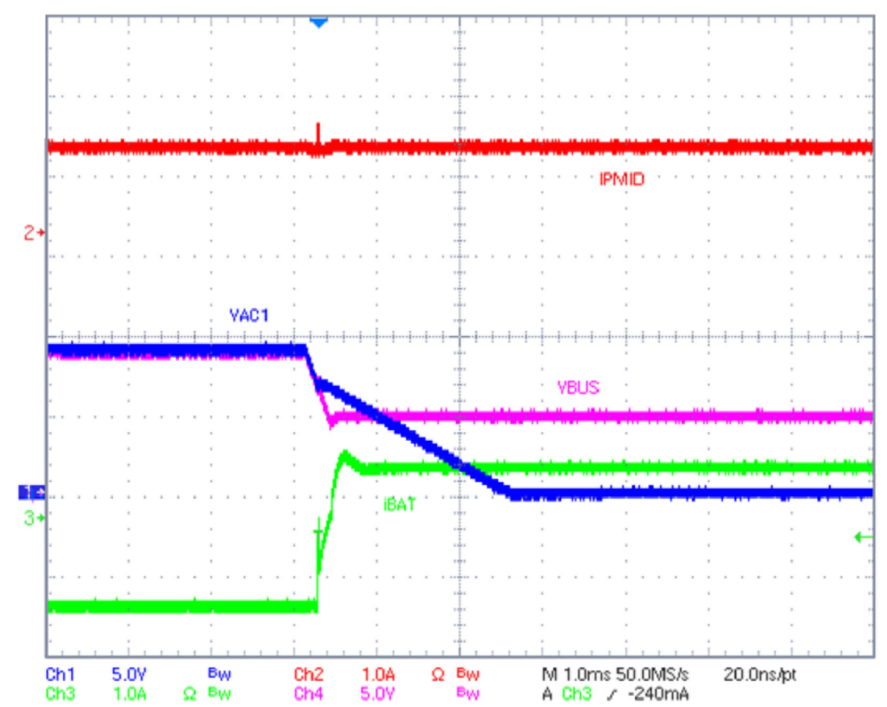
Figure 4 shows the tested waveforms of the charger backup mode for FRS. A 9-V adapter is connected at USB1 as the input power. VBUS is shorted to the adapter by turning on ACFET1-
RBFET1. Assume that there is a 1-A accessory current at PMID and a 1-A charging current at BAT. When the 9-V adapter voltage (VAC) is gone, the PMID and VBUS can still be regulated at 5 V to continuously power the 1-A PMID load.
 Figure 4 Buck-boost charger FRS from
VBUS sink to VBUS source.