SNAA396 February 2024 LMK5B33216 , LMK5B33414
2 LMK5B33216 for SerDes Applications
Designed for SerDes applications, the LMK5B33216 is a high-performance network synchronizer that meets the stringent Ethernet-based networking requirements for jitter, rise or fall time, hitless switching, and holdover.
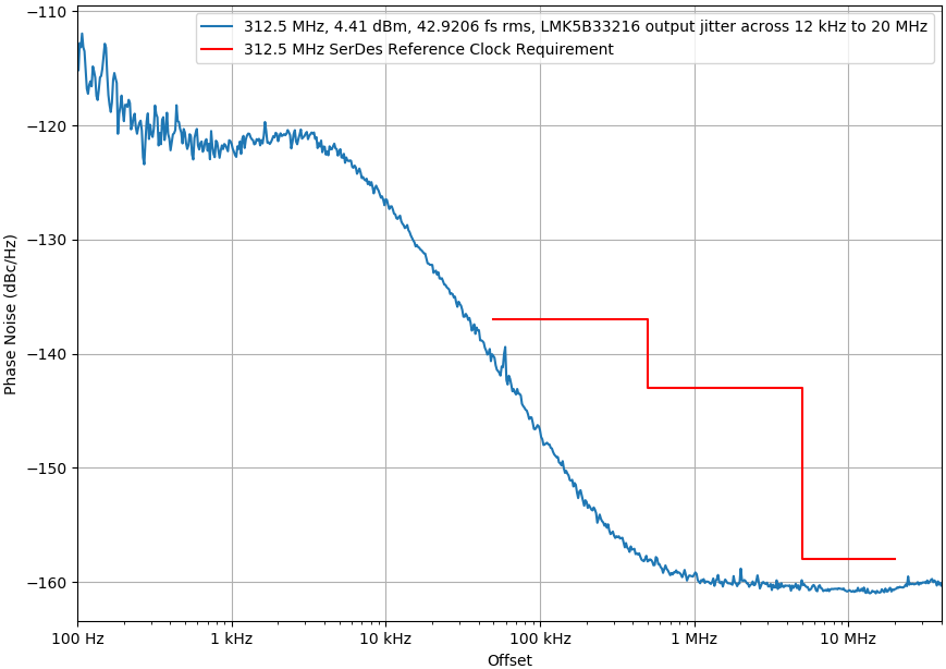
Table 2-1 compares the performance of the LMK5B33216 with an example SerDes core reference clock used for 800G switch applications. The LMK5B33216 meets and exceeds the requirements of the reference example clock.
| Parameter | Example SerDes Core Reference Clock | LMK5B33216(1) | UNIT | ||||
|---|---|---|---|---|---|---|---|
| MIN | TYP | MAX | MIN | TYP | MAX | ||
| Frequency | — | 312.5 | — | — | 312.5 | — | MHz |
| RMS jitter (12kHz to 20MHz) | — | — | 90 | — | 42(2) | 60(2) | fs |
| Reference clock phase noise at 100kHz | — | — | -137 | — | -146 | — | dBc/Hz |
| Reference clock phase noise at 1MHz | — | — | -143 | — | -159 | — | dBc/Hz |
| Reference clock phase noise at 10MHz | — | — | -158 | — | -160 | — | dBc/Hz |
| Differential peak-to-peak voltage swing | 500 | — | 1800 | 670 | — | 2300 | mVpp |
| Rise or fall time (20% to 80%) | — | 300 | 400 | 175 | 230 | 300 | ps |
| Operating ambient temperature | — | — | — | -40 | — | 85 | °C |
 Figure 2-1 LMK5B33216 Output Phase Noise and Jitter for 312.5MHz (using a 48MHz XO input)
Bit error rates (BER) are minimized in applications involving high-speed SerDes links with the excellent jitter performance of the LMK5B33216. The LMK5B33216, along with the TI PTP Stack option, achieves better than Class D accuracy (with sub 5ns timing accuracy). This accuracy meets ITU-T standards like G8275.1 and G8275.2 for full timing and partial timing support. For more information on TI’s complete IEEE-1588 PTP and SyncE clocking options, visit TI's Clocks and Timing page.
TI’s network synchronizers leverage a Digital Phase-Locked Loop (DPLL) and an Analog Phase-Locked Loop (APLL) combination to maintain phase lock with a reference clock. The DPLL steers the clock output phase by making continuous updates to the APLL numerator as the DPLL tracks the phase of the reference clock. The LMK5B33216 contains three pairs of DPLL + APLL to support up to three synchronization and frequency domains, as illustrated in the block diagram in Figure 2-2.
The clock outputs can phase-lock between two inputs (LMK5B33216) or four inputs (LMK5B33414) when using the DPLL + APLL. Alternatively, the outputs can lock to a single reference, or oscillator, when using only the APLL. The device can operate in three modes: normal operation with the DPLL active, holdover when the input clocks are unavailable, and free-run where the DPLL is turned off and only the internal APLL is functioning.
Additionally, the LMK5B33216 provides input clock detection and monitoring, wander and jitter filtering, hitless switching, holdover, and Zero-Delay Mode (ZDM) functionality. Each DPLL includes a programmable loop bandwidth (LBW) to maximize flexibility and ease of use, which can be set between 1MHz to 4kHz without external loop filter components. The APLL loop filter is fully integrated except for one external capacitor.
The LMK5B33216 clock outputs are configurable from several output formats: 1.8V or 2.65V LVCMOS, HCSL, and LVDS/HSDS (High Swing Differential Signaling). The output swing and common-mode voltage are programmable to meet various receiver requirements with the HSDS format.
 Figure 2-2 LMK5B33216 Functional Block Diagram