SNAS680E December   2015  – August 2022 LMX2582

PRODUCTION DATA  

  1. Features
  2. Applications
  3. Description
  4. Revision History
  5. Pin Configuration and Functions
  6. Specifications
    1. 6.1 Absolute Maximum Ratings
    2. 6.2 ESD Ratings
    3. 6.3 Recommended Operating Conditions
    4. 6.4 Thermal Information
    5. 6.5 Electrical Characteristics
    6. 6.6 Timing Requirements
    7. 6.7 Typical Characteristics
  7. Detailed Description
    1. 7.1 Overview
    2. 7.2 Functional Block Diagram
    3. 7.3 Functional Description
      1. 7.3.1  Input Signal
      2. 7.3.2  Input Signal Path
      3. 7.3.3  PLL Phase Detector and Charge Pump
      4. 7.3.4  N Divider and Fractional Circuitry
      5. 7.3.5  Voltage Controlled Oscillator
      6. 7.3.6  VCO Calibration
      7. 7.3.7  Channel Divider
      8. 7.3.8  Output Distribution
      9. 7.3.9  Output Buffer
      10. 7.3.10 Phase Adjust
    4. 7.4 Device Functional Modes
      1. 7.4.1 Power Down
      2. 7.4.2 Lock Detect
      3. 7.4.3 Register Readback
    5. 7.5 Programming
      1. 7.5.1 Recommended Initial Power on Programming Sequence
      2. 7.5.2 Recommended Sequence for Changing Frequencies
    6. 7.6 Register Maps
      1. 7.6.1 LMX2582 Register Map – Default Values
        1. 7.6.1.1 Register Descriptions
  8. Application and Implementation
    1. 8.1 Application Information
      1. 8.1.1  Optimization of Spurs
        1. 8.1.1.1 Understanding Spurs by Offsets
        2. 8.1.1.2 Spur Mitigation Techniques
      2. 8.1.2  Configuring the Input Signal Path
        1. 8.1.2.1 Input Signal Noise Scaling
      3. 8.1.3  Input Pin Configuration
      4. 8.1.4  Using the OSCin Doubler
      5. 8.1.5  Using the Input Signal Path Components
        1. 8.1.5.1 Moving Phase Detector Frequency
        2. 8.1.5.2 Multiplying and Dividing by the Same Value
      6. 8.1.6  Designing for Output Power
      7. 8.1.7  Current Consumption Management
      8. 8.1.8  Decreasing Lock Time
      9. 8.1.9  Modeling and Understanding PLL FOM and Flicker Noise
      10. 8.1.10 External Loop Filter
    2. 8.2 Typical Application
      1. 8.2.1 Design for Low Jitter
        1. 8.2.1.1 Design Requirements
        2. 8.2.1.2 Detailed Design Procedure
        3. 8.2.1.3 Application Curve
    3. 8.3 Power Supply Recommendations
    4. 8.4 Layout
      1. 8.4.1 Layout Guidelines
      2. 8.4.2 Layout Example
  9. Device and Documentation Support
    1. 9.1 Device Support
      1. 9.1.1 Development Support
    2. 9.2 Documentation Support
      1. 9.2.1 Related Documentation
    3. 9.3 Receiving Notification of Documentation Updates
    4. 9.4 Support Resources
    5. 9.5 Trademarks
    6. 9.6 Electrostatic Discharge Caution
    7. 9.7 Glossary
  10. 10Mechanical, Packaging, and Orderable Information

Moving Phase Detector Frequency

Engaging the multiplier in the reference path allows more flexibility in setting the PFD frequency. One example use case of this is if Fvco % Fpd is the dominant spur. This method can move the PFD frequency and thus the Fvco % Fpd.

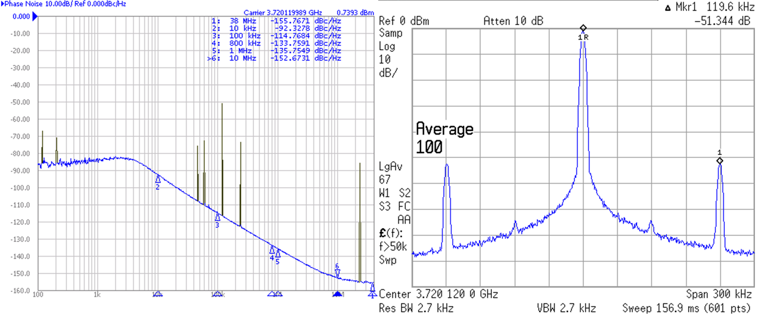
Example: Fvco = 3720.12 MHz, Fosc = 300 MHz, Pre-R divider = 5, Fpd = 60 MHz, Fvco%Fosc = 120.12 MHz (Far out), Fvco%Fpd = 120 kHz (dominant). There is a Fvco%Fpd spur at 120 kHz (refer to Figure 8-5).
GUID-7E480620-04E6-49C2-AB6D-BACF0B052D54-low.png Figure 8-5 Fvco % Fpd Spur

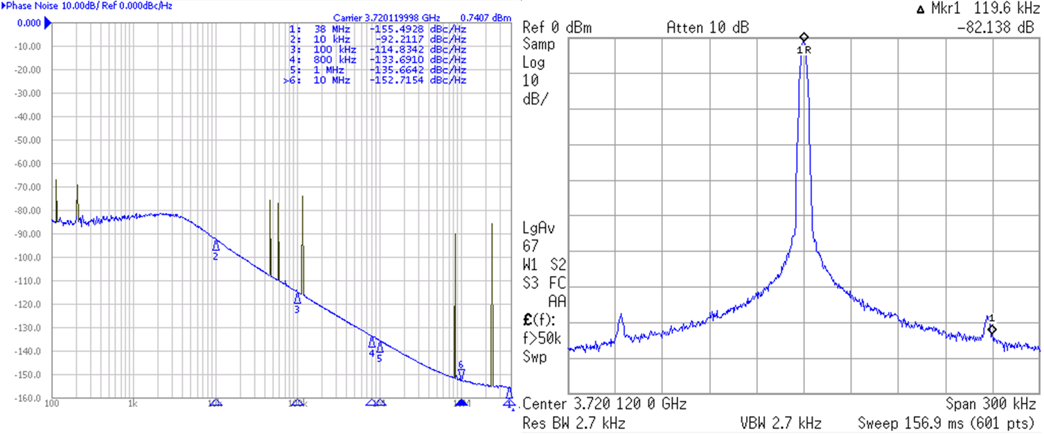
Then second case, using divider and multiplier, is Fpd = 53.57 MHz away from 120-kHz spur. Fvco = 3720.12MHz, Fosc = 300MHz, Pre-R divider = 7, Multiplier = 5, Post-R divider = 4, Fpd = 53.57 MHz, Fvco%Fosc = 120.12 MHz (Far out). Fvco % Fpd = 23.79 MHz (far out). There is a 20–dB reduction for the Fvco % Fpd spur at 120 kHz (refer to Figure 8-6).
GUID-42D83020-B959-4075-B59B-6C09E2B90681-low.png Figure 8-6 Moving Away From Fvco % Fpd Spur