SNAS680E December 2015 – August 2022 LMX2582
PRODUCTION DATA
- 1 Features
- 2 Applications
- 3 Description
- 4 Revision History
- 5 Pin Configuration and Functions
- 6 Specifications
- 7 Detailed Description
-
8 Application and Implementation
- 8.1
Application Information
- 8.1.1 Optimization of Spurs
- 8.1.2 Configuring the Input Signal Path
- 8.1.3 Input Pin Configuration
- 8.1.4 Using the OSCin Doubler
- 8.1.5 Using the Input Signal Path Components
- 8.1.6 Designing for Output Power
- 8.1.7 Current Consumption Management
- 8.1.8 Decreasing Lock Time
- 8.1.9 Modeling and Understanding PLL FOM and Flicker Noise
- 8.1.10 External Loop Filter
- 8.2 Typical Application
- 8.3 Power Supply Recommendations
- 8.4 Layout
- 8.1
Application Information
- 9 Device and Documentation Support
- 10Mechanical, Packaging, and Orderable Information
6.6 Timing Requirements
3.15 V ≤ VCC ≤ 3.45 V, –40°C ≤ TA ≤ 85°C, except as specified. Typical values are at VCC = 3.3 V, TA = 25°C
| MIN | TYP | MAX | UNIT | |||
|---|---|---|---|---|---|---|
| MICROWIRE TIMING | ||||||
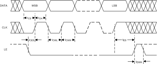
| tES | Clock to enable low time | See Figure 6-1 | 5 | ns | ||
| tCS | Data to clock setup time | 2 | ns | |||
| tCH | Data to clock hold time | 2 | ns | |||
| tCWH | Clock pulse width high | 5 | ns | |||
| tCWL | Clock pulse width low | 5 | ns | |||
| tCES | Enable to clock setup time | 5 | ns | |||
| tEWH | Enable pulse width high | 2 | ns | |||
 Figure 6-1 Serial Data Input Timing Diagram
There are several considerations for programming:
- A slew rate of at least 30 V/µs is recommended for the CLK, DATA, LE
- The DATA is clocked into a shift register on each rising edge of the CLK signal. On the rising edge of the last CLK signal, the data is sent from the shift registers to a register bank
- The LE pin may be held high after programming and clock pulses are ignored
- When CLK and DATA lines are shared between devices, TI recommends diving down the voltage to the CLK, DATA, and LE pins closer to the minimum voltage. This provides better noise immunity
- If the CLK and DATA lines are toggled while the VCO is in lock, as is sometimes the case when these lines are shared with other parts, the phase noise may be degraded during the time of this programming