SNAU210B March 2020 – July 2021
- Trademarks
- 1Evaluation Board Setup
- 2EVM Description
- 3Bringing LMX2594 to a Lock State
- 4Loop Filter Configuration
- 5Key Results to Expect
- A Schematic
- B Bill of Materials
- C Board Layers Stack-Up
- D Changing Reference Oscillator and Setup
- E Connecting Reference Pro
- F Ramping Feature
- G SYSREF Feature
- H Enabling Onboard DC-DC Buck Converter (TPS62150)
- Revision History
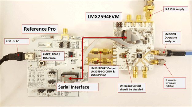
E Connecting Reference Pro
To use Reference Pro, change the configuration for SE or differential connection as shown on Section D.
 Figure E-1 LMX2594EVM Setup With
Reference Pro
Figure E-1 LMX2594EVM Setup With
Reference ProThe LMK61PD0A2 has several control pins dedicated for output format control, output frequency control, and output enable control. These control pins can be configured through the jumpers shown in Table E-1 and Table E-2.
Jumpers FS1, FS0, OS, and OE can be used to configure the corresponding control pin to either high or low state by strapping the center pin to VDD position (tie pins 2-3) or GND position (tie pins 1-2), respectively. Connections from the VDD position to the device supply or from the GND position to the ground plane are connected by 1.5-kΩ resistors.
| FS1 | FS0 | OUTPUT FREQUENCY (MHz) |
|---|---|---|
| 0 | 0 | 100 |
| 0 | NC | 312.5 |
| 0 | 1 | 125 |
| NC | 0 | 106.25 |
| NC | NC | 156.25 |
| NC | 1 | 212.5 |
| 1 | 0 | 62.5 |
| OS | OE | OUTPUT TYPE |
|---|---|---|
| X | O | Disabled (PLL Functional) |
| 0 | 1 | LVPECL |
| NC | 1 | LVDS |
| 1 | 1 | HCSL |
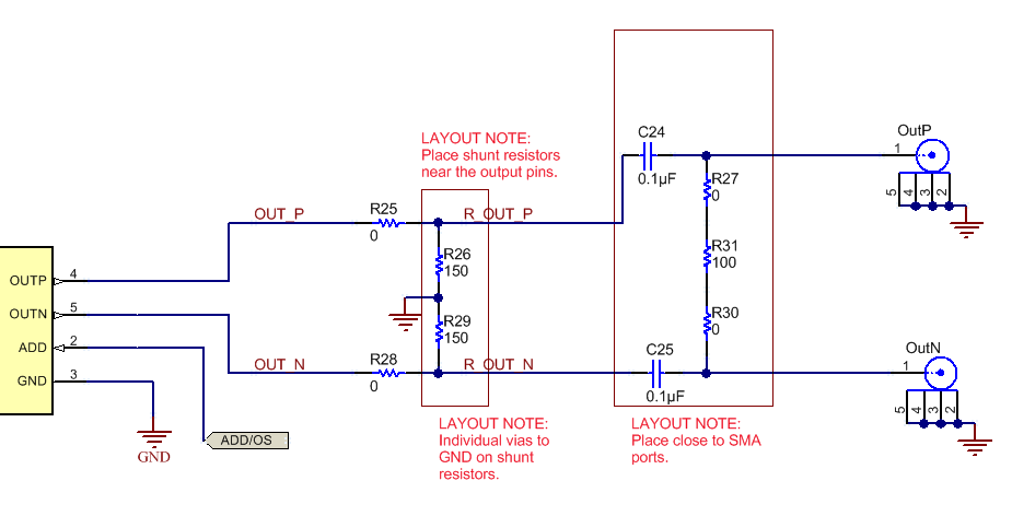
The OS pin is used to bias internal drivers and change the output type. It is imperative to match the output termination passive components as shown on Table E-3 with the output type from Table E-2.
Table E-3 lists component values for each configuration.
| OUTPUT FORMAT | COUPLING | COMPONENT | VALUE |
|---|---|---|---|
| LVPECL | AC (default EVM configuration) |
R25, R28 | 0 Ω |
| R26, R29 | 150 Ω | ||
| C24, C25 | 0.01 µF | ||
| R27, R30, R31 | DNP | ||
| DC(1) | R25, R28, C24, C25 | 0 Ω | |
| R26, R29, R27, R30, R31 | DNP | ||
| LVDS(2) | AC | R25, R28, R27, R30 | 0 Ω |
| R31 | 100 Ω | ||
| C24, C25 | 0.01 µF | ||
| R26, R29 | DNP | ||
| DC | R25, R27, R28, R30, C24, C25 | 0 Ω | |
| R31 | 100 Ω | ||
| R26, R29 | DNP | ||
| HCSL | AC | R25, R28 | 0 Ω |
| R26, R29 | 50 Ω | ||
| C24, C25 | 0 Ω | ||
| R27, R30, R31 | DNP | ||
| DC | R25, R28 | 0 Ω | |
| R26, R29 | 50 Ω | ||
| C24, C25 | 0.01 µF | ||
| R27. R30, R31 | DNP |
 Figure E-2 LMK61PD0A2 Output
Termination