SNAU259 August 2021 LMK1D1208
5 Power Supply Connection
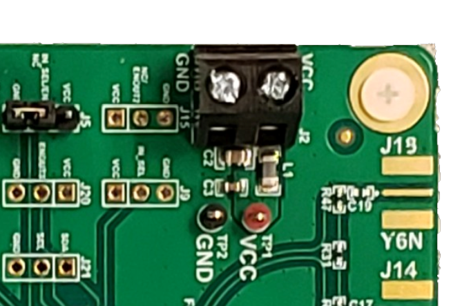
 Figure 5-1 Power Block Connection .
TP1 and TP2 can be used as optional test points.
A supply voltage of 1.71 V to 3.465 V can be used for this EVM.
SNAU259 August 2021 LMK1D1208
 Figure 5-1 Power Block Connection .
TP1 and TP2 can be used as optional test points.
A supply voltage of 1.71 V to 3.465 V can be used for this EVM.