SNAU268 June 2021 LMK1C1104
5 Enabling/Disabling the Outputs
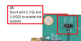
The enable pin, 1G, of the LMK1C1104DQF can be controlled using jumper J3. Pull 1G to VDD by shunting pins 2 and 3 of J3 to enable the outputs as shown in Figure 5-1. Leave 1G floating or pull to GND to disable the outputs.
 Figure 5-1 J3 Jumper Location.
 By default, a shunt is placed on pins 2 and 3 to enable the outputs.