SNOA961A February   2017  – February 2023 LDC2112 , LDC2114 , LDC3114 , LDC3114-Q1


  1.   Inductive Touch System Design Guide for HMI Button Applications
  2. 1Mechanical Design
    1. 1.1 Theory of Operation
    2. 1.2 Button Construction
    3. 1.3 Mechanical Deflection
    4. 1.4 Mechanical Factors that Affect Sensitivity
      1. 1.4.1 Target Material Selection
        1. 1.4.1.1 Material Stiffness
        2. 1.4.1.2 Material Conductivity
      2. 1.4.2 Button Geometry
      3. 1.4.3 Spacing Between Target and Sensor
    5. 1.5 Layer Stacks of Touch Buttons
      1. 1.5.1 Conductive Surface
      2. 1.5.2 Non-Conductive Surface
    6. 1.6 Sensor Mounting Reference
    7. 1.7 Sensor Mounting Techniques
      1. 1.7.1 Adhesive-Based
      2. 1.7.2 Spring-Based
      3. 1.7.3 Slot-Based
    8. 1.8 Mechanical Isolation
  3. 2Sensor Design
    1. 2.1 Overview
      1. 2.1.1 Sensor Electrical Parameters
      2. 2.1.2 Sensor Frequency
      3. 2.1.3 Sensor RP and RS
      4. 2.1.4 Sensor Inductance
      5. 2.1.5 Sensor Capacitance
      6. 2.1.6 Sensor Quality Factor
    2. 2.2 Inductive Touch
    3. 2.3 LDC211x/LDC3114 Design Boundary Conditions
    4. 2.4 Sensor Physical Construction
      1. 2.4.1 Sensor Physical Size
      2. 2.4.2 Sensor Capacitor Position
      3. 2.4.3 Shielding INn traces
      4. 2.4.4 Shielding Capacitance
      5. 2.4.5 CCOM Sizing
      6. 2.4.6 Multi-Layer Design
        1. 2.4.6.1 Sensor Parasitic Capacitance
      7. 2.4.7 Sensor Spacers
      8. 2.4.8 Sensor Stiffener
      9. 2.4.9 Racetrack Inductor Shape
    5. 2.5 Example Sensor
  4. 3Summary
  5. 4Revision History

Conductive Surface

If the touch button is implemented on a conductive surface, such as aluminum or stainless steel, the surface can be used as the target of detection. In this configuration, the metal target is at the top of the entire stack. The user directly presses the metal target, causing a micro-deflection in the metal itself. The metal deflection will cause a change in the inductance of the sensor coil.
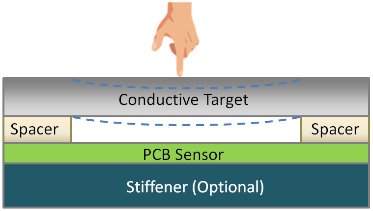
GUID-38D0451F-97B2-4952-9C6D-63E35E19219C-low.pngFigure 1-7 Example Layer Stack With Conductive Surface