SNOSD82D June   2018  – September 2022 TMP117

PRODUCTION DATA  

  1. Features
  2. Applications
  3. Description
  4. Revision History
  5. Pin Configuration and Functions
  6. Specifications
    1. 6.1 Absolute Maximum Ratings
    2. 6.2 ESD Ratings
    3. 6.3 Recommended Operating Conditions
    4. 6.4 Thermal Information
    5. 6.5 Electrical Characteristics
    6. 6.6 Switching Characteristics
    7. 6.7 Two-Wire Interface Timing
    8. 6.8 Timing Diagram
    9. 6.9 Typical Characteristics
  7. Detailed Description
    1. 7.1 Overview
    2. 7.2 Functional Block Diagrams
    3. 7.3 Feature Description
      1. 7.3.1 Power Up
      2. 7.3.2 Averaging
      3. 7.3.3 Temperature Result and Limits
    4. 7.4 Device Functional Modes
      1. 7.4.1 Continuous Conversion Mode
      2. 7.4.2 Shutdown Mode (SD)
      3. 7.4.3 One-Shot Mode (OS)
      4. 7.4.4 Therm and Alert Modes
        1. 7.4.4.1 Alert Mode
        2. 7.4.4.2 Therm Mode
    5. 7.5 Programming
      1. 7.5.1 EEPROM Programming
        1. 7.5.1.1 EEPROM Overview
        2. 7.5.1.2 Programming the EEPROM
      2. 7.5.2 Pointer Register
      3. 7.5.3 I2C and SMBus Interface
        1. 7.5.3.1 Serial Interface
          1. 7.5.3.1.1 Bus Overview
          2. 7.5.3.1.2 Serial Bus Address
          3. 7.5.3.1.3 Writing and Reading Operation
          4. 7.5.3.1.4 Slave Mode Operations
            1. 7.5.3.1.4.1 Slave Receiver Mode
            2. 7.5.3.1.4.2 Slave Transmitter Mode
          5. 7.5.3.1.5 SMBus Alert Function
          6. 7.5.3.1.6 General-Call Reset Function
          7. 7.5.3.1.7 Timeout Function
          8. 7.5.3.1.8 Timing Diagrams
    6. 7.6 Register Map
  8. Application and Implementation
    1. 8.1 Application Information
    2. 8.2 Typical Application
      1. 8.2.1 Design Requirements
      2. 8.2.2 Detailed Design Procedure
        1. 8.2.2.1 Noise and Averaging
        2. 8.2.2.2 Self-Heating Effect (SHE)
        3. 8.2.2.3 Synchronized Temperature Measurements
      3. 8.2.3 Application Curves
  9. Power Supply Recommendations
  10. 10Layout
    1. 10.1 Layout Guidelines
    2. 10.2 Layout Examples
  11. 11Device and Documentation Support
    1. 11.1 Documentation Support
      1. 11.1.1 Related Documentation
    2. 11.2 Receiving Notification of Documentation Updates
    3. 11.3 Support Resources
    4. 11.4 Trademarks
    5. 11.5 Electrostatic Discharge Caution
    6. 11.6 Glossary
  12. 12Mechanical, Packaging, and Orderable Information

Typical Characteristics

at TA = 25°C, V+ = 3.3 V, and measurement taken in oil bath (unless otherwise noted)
GUID-88D0F2FC-EA43-4318-9665-0B89963CCEA6-low.gif
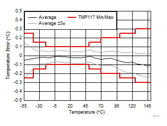
1-Hz conversion cycle, 8 averages mode
Figure 6-2 DRV Package Temperature Error vs Temperature
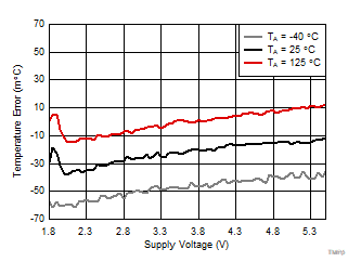
GUID-995E60F7-36C3-47F5-BF2F-BDE238083A8B-low.gifFigure 6-4 Temperature Error vs Supply Voltage
GUID-46A20B95-69F1-45EE-817A-7ABA6057E1E5-low.gif


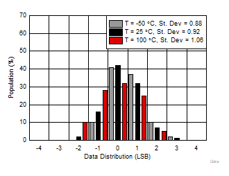
Figure 6-6 Data Reading Distribution Over Temperature (No Averaging, V+ = 3.3 V)
GUID-E62D9BBE-E2E8-42CC-A6A0-B3DD96C185AC-low.gif
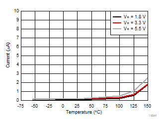
Serial bus inactive
Figure 6-8 Quiescent Current in Shutdown Mode
GUID-88FDF03C-D655-4264-9363-DE2C2DB64E42-low.gif
SCL pin clocked
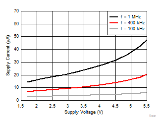
Figure 6-10 Quiescent Current in Shutdown Mode
GUID-20201022-CA0I-9GGK-WDB3-WRD0GD35DKQ7-low.gif


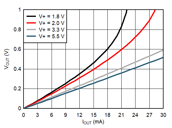
Figure 6-12 ALERT Pin Output Voltage vs Pin Sink Current
GUID-95F4013A-5C95-4C99-A062-FF92881D10F9-low.gif
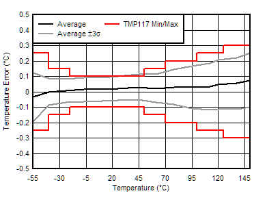
1-Hz conversion cycle, 8 averages mode
Figure 6-3 YBG Package Temperature Error vs Temperature
GUID-77F3C36C-174D-4DAD-86F6-81E9854431E3-low.gif
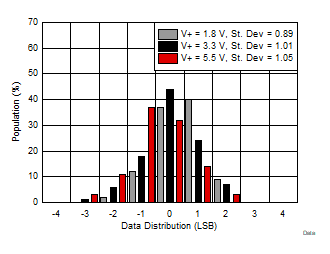
Figure 6-5 Data Reading Distribution Over Supply Voltage (No Averaging)
GUID-E82F1741-0E51-46CC-9F8D-10BDB7A8E98C-low.gif
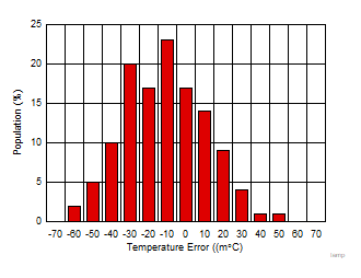
TA = 25 °C. V+ = 3.3 V. One-shot mode with averaging = 8.
Figure 6-7 Typical Temperature Distribution Error
GUID-6AC7C6EC-CBCC-41B0-A232-718723056D59-low.gif
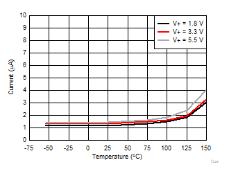
Serial bus inactive
Figure 6-9 Quiescent Current in Standby Mode
GUID-F2B26275-8B13-4258-A7F9-3977AFB39C99-low.gif
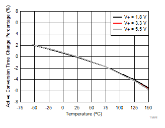
Normalized to 25°C and V+ = 3.3 V
Figure 6-11 Active Conversion Time vs Temperature
GUID-5374C2EF-7682-4A5A-8F62-21F8F28083C9-low.gif
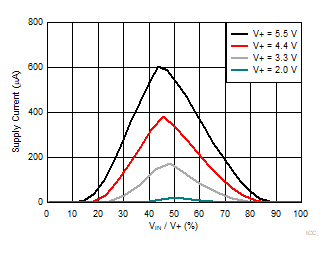
Input voltage of SCL, SDA, or ADD0 pin
Figure 6-13 Supply Current vs Input Cell Voltage