SNOSD82D June 2018 – September 2022 TMP117
PRODUCTION DATA
- 1 Features
- 2 Applications
- 3 Description
- 4 Revision History
- 5 Pin Configuration and Functions
- 6 Specifications
-
7 Detailed Description
- 7.1 Overview
- 7.2 Functional Block Diagrams
- 7.3 Feature Description
- 7.4 Device Functional Modes
- 7.5
Programming
- 7.5.1 EEPROM Programming
- 7.5.2 Pointer Register
- 7.5.3 I2C and SMBus Interface
- 7.6 Register Map
- 8 Application and Implementation
- 9 Power Supply Recommendations
- 10Layout
- 11Device and Documentation Support
- 12Mechanical, Packaging, and Orderable Information
7.4.4.1 Alert Mode
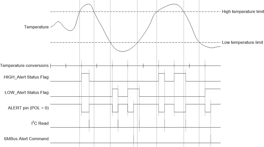
When the T/nA bit in the configuration register is set to 0, the device is in alert mode. In this mode, the device compares the conversion result at the end of every conversion with the values in the low limit register and high limit register. If the temperature result exceeds the value in the high limit register, the HIGH_Alert status flag in the configuration register is set. On the other hand, if the temperature result is lower than the value in the low limit register, the LOW_Alert status flag in the configuration register is set. As shown in Figure 7-5, the user can run an I2C read from the configuration register to clear the status flags in alert mode.
When a user configures the device in alert mode, it affects the behavior of the ALERT pin. The device asserts the ALERT pin in this mode when either the HIGH_Alert or the LOW_Alert status flag is set, as shown in Figure 7-5. The user can either run an I2C read of the configuration register (which also clears the status flags) or run an SMBus alert response command (see the Section 7.5.3.1.5 section) to deassert the ALERT pin. The polarity of the ALERT pin can be changed by using the POL bit setting in the configuration register.
This mode effectively makes the device behave like a window limit detector. Thus this mode can be used in applications where detecting if the temperature goes outside of the specified range is necessary.
 Figure 7-5 Alert Mode Timing Diagram