SNOSD82D June   2018  – September 2022 TMP117

PRODUCTION DATA  

  1. Features
  2. Applications
  3. Description
  4. Revision History
  5. Pin Configuration and Functions
  6. Specifications
    1. 6.1 Absolute Maximum Ratings
    2. 6.2 ESD Ratings
    3. 6.3 Recommended Operating Conditions
    4. 6.4 Thermal Information
    5. 6.5 Electrical Characteristics
    6. 6.6 Switching Characteristics
    7. 6.7 Two-Wire Interface Timing
    8. 6.8 Timing Diagram
    9. 6.9 Typical Characteristics
  7. Detailed Description
    1. 7.1 Overview
    2. 7.2 Functional Block Diagrams
    3. 7.3 Feature Description
      1. 7.3.1 Power Up
      2. 7.3.2 Averaging
      3. 7.3.3 Temperature Result and Limits
    4. 7.4 Device Functional Modes
      1. 7.4.1 Continuous Conversion Mode
      2. 7.4.2 Shutdown Mode (SD)
      3. 7.4.3 One-Shot Mode (OS)
      4. 7.4.4 Therm and Alert Modes
        1. 7.4.4.1 Alert Mode
        2. 7.4.4.2 Therm Mode
    5. 7.5 Programming
      1. 7.5.1 EEPROM Programming
        1. 7.5.1.1 EEPROM Overview
        2. 7.5.1.2 Programming the EEPROM
      2. 7.5.2 Pointer Register
      3. 7.5.3 I2C and SMBus Interface
        1. 7.5.3.1 Serial Interface
          1. 7.5.3.1.1 Bus Overview
          2. 7.5.3.1.2 Serial Bus Address
          3. 7.5.3.1.3 Writing and Reading Operation
          4. 7.5.3.1.4 Slave Mode Operations
            1. 7.5.3.1.4.1 Slave Receiver Mode
            2. 7.5.3.1.4.2 Slave Transmitter Mode
          5. 7.5.3.1.5 SMBus Alert Function
          6. 7.5.3.1.6 General-Call Reset Function
          7. 7.5.3.1.7 Timeout Function
          8. 7.5.3.1.8 Timing Diagrams
    6. 7.6 Register Map
  8. Application and Implementation
    1. 8.1 Application Information
    2. 8.2 Typical Application
      1. 8.2.1 Design Requirements
      2. 8.2.2 Detailed Design Procedure
        1. 8.2.2.1 Noise and Averaging
        2. 8.2.2.2 Self-Heating Effect (SHE)
        3. 8.2.2.3 Synchronized Temperature Measurements
      3. 8.2.3 Application Curves
  9. Power Supply Recommendations
  10. 10Layout
    1. 10.1 Layout Guidelines
    2. 10.2 Layout Examples
  11. 11Device and Documentation Support
    1. 11.1 Documentation Support
      1. 11.1.1 Related Documentation
    2. 11.2 Receiving Notification of Documentation Updates
    3. 11.3 Support Resources
    4. 11.4 Trademarks
    5. 11.5 Electrostatic Discharge Caution
    6. 11.6 Glossary
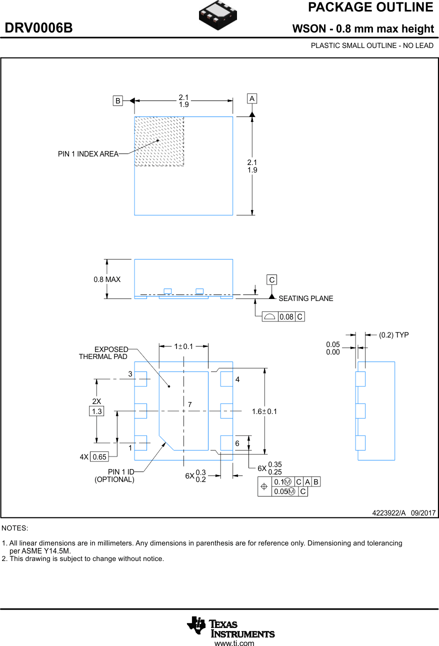
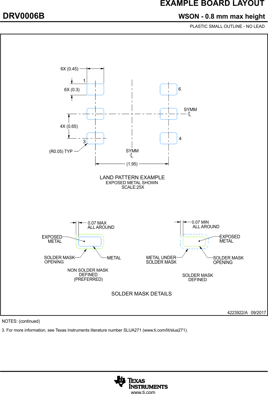
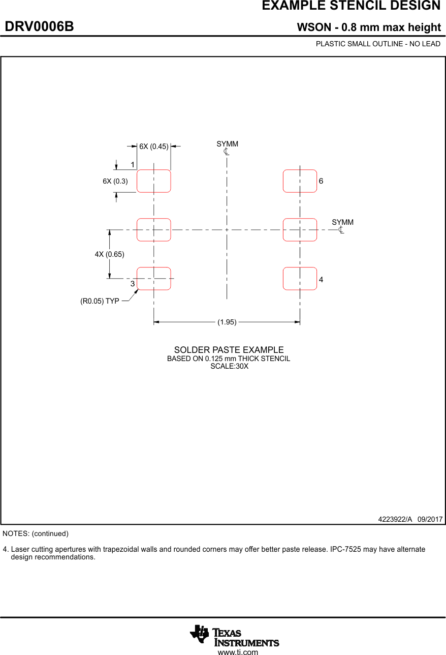
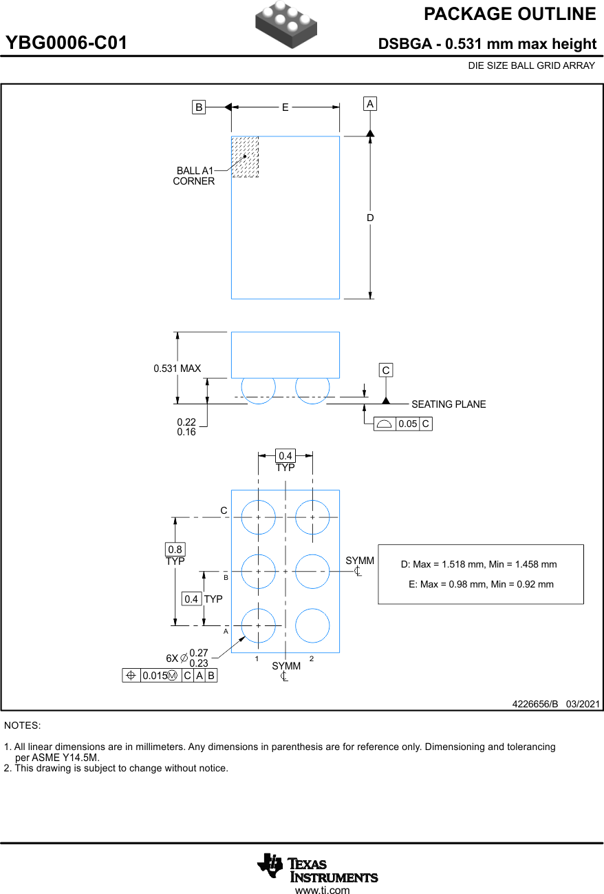
  12. 12Mechanical, Packaging, and Orderable Information
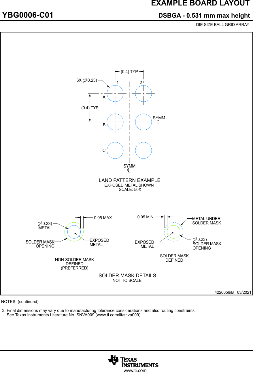
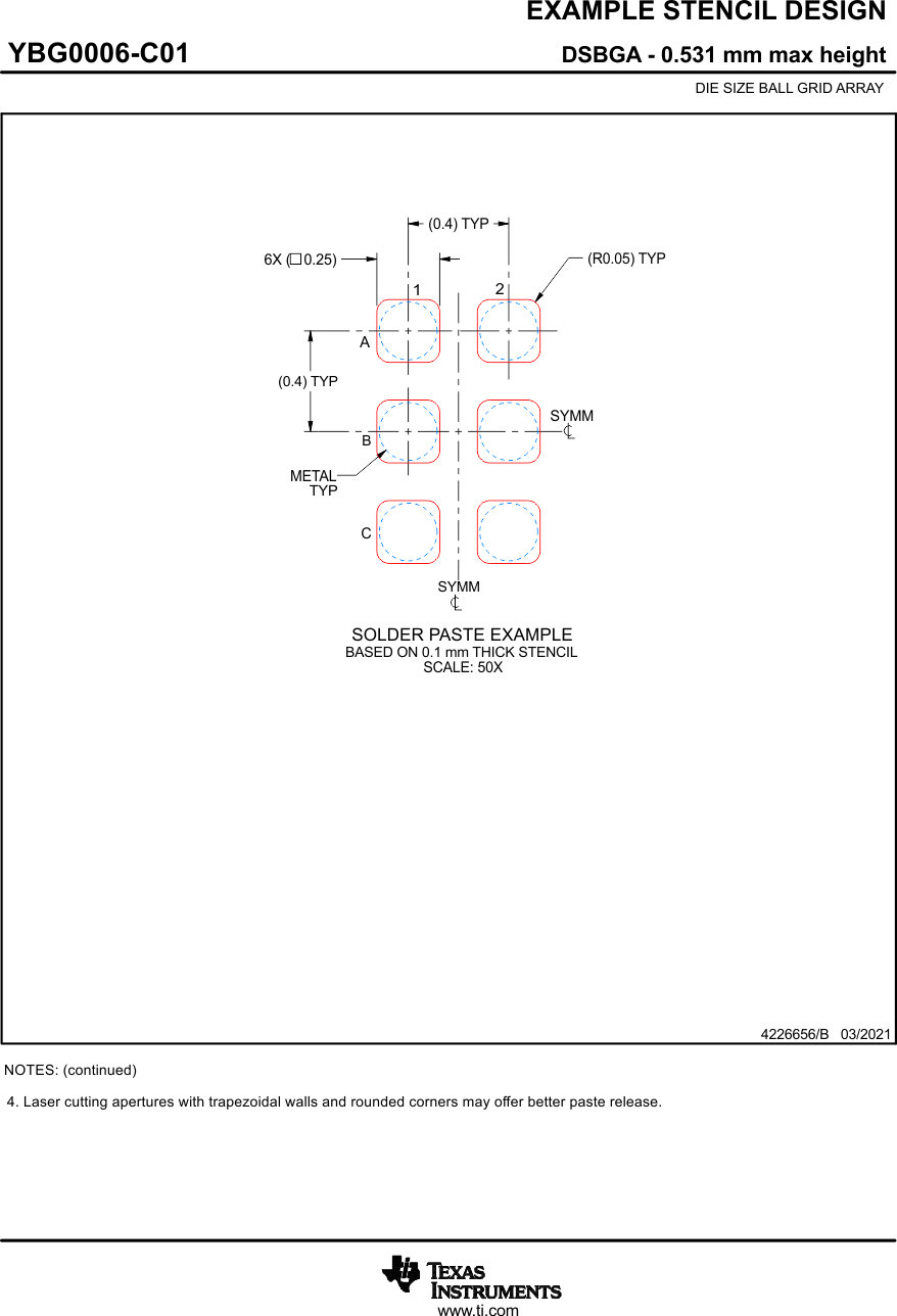
Mechanical, Packaging, and Orderable Information

The following pages include mechanical, packaging, and orderable information. This information is the most current data available for the designated devices. This data is subject to change without notice and revision of this document. For browser-based versions of this data sheet, refer to the left-hand navigation.


GUID-20210324-CA0I-LGB2-WDTF-6NZ6NBCRLXFH-low.gif

GUID-20210324-CA0I-NPMF-TJNH-FQVP653MW1B3-low.gif

GUID-20210324-CA0I-HTGP-L4GH-VHGQBSWRSMM8-low.gif

GUID-20210312-CA0I-RT76-GLNH-XBXJXG47392S-low.gif

GUID-20210312-CA0I-FPBC-NHB4-D6D3ZSQFWL1L-low.gif

GUID-20210312-CA0I-HX4M-KF71-DTJHDT2HSKFR-low.gif