SNVA866A February 2019 – January 2023 LM5155 , LM5155-Q1 , LM51551 , LM51551-Q1
- How to design an Isolated Flyback using LM5155
- Trademarks
- 1Introduction
- 2Example Application
- 3Calculations and Component Selection
- 4Component Selection Summary
- 5Small Signal Frequency Analysis
- 6Revision History
3.4 MOSFET Selection
MOSFET selection for a flyback controller focuses on power dissipation and voltage rating. Power dissipation of MOSFET is composed of two different parts, conduction losses and switching losses. Conduction losses are dominated by the RDS(ON) resistance of the MOSFET. Switching losses occur during the rise time and fall time of the switch node, when the N-channel MOSFET is turning on and turning off. During the rise time and fall time, current through the MOSFET channel and a large voltage drop across the drain to source are present, resulting in power dissipation. The longer the rise and fall time of the switch node the higher the switching losses. Selecting a MOSFET with minimal parasitic capacitances decreases the switching losses.
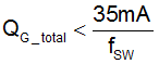
The total gate charge (QG_total) must be small enough to keep the internal VCC regulator from entering current limit. The QG_total for a given MOSFET can be found in the component data sheet. Equation 16 provides the maximum total gate charge of the MOSFET for the selected switching frequency. The QG_total of the selected MOSFET is 35nC.
The RMS current of the MOSFET is estimated using Equation 17. By estimating the switch RMS current, a MOSFET with an adequately small RDS(ON) value is selected.
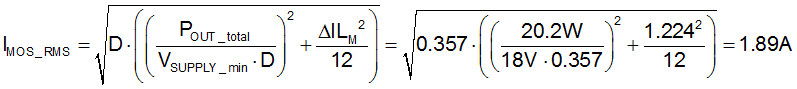
The RDS(ON) of the selected MOSFET is 8.7mΩ.
The drain to source break down voltage rating on the MOSFET needs to be higher than the reflected secondary side voltage plus the maximum input voltage as calculated in Equation 18.
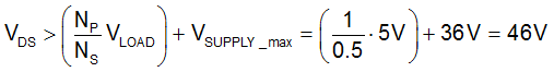
Due to the parasitic leakage inductance of the primary winding, the switch node voltage rings well above the value calculated in Equation 18. To overcome the ringing on the switch node a voltage clamp can be added. Designing this clamp is not described in this application report. For this design a MOSFET with a voltage rating of 100 V is selected.